- 您現(xiàn)在的位置:買賣IC網(wǎng) > PDF目錄225572 > XC4VFX100-10FFG1517I (XILINX INC) FPGA, 10544 CLBS, 1028 MHz, PBGA1517 PDF資料下載
參數(shù)資料
| 型號: | XC4VFX100-10FFG1517I |
| 廠商: | XILINX INC |
| 元件分類: | FPGA |
| 英文描述: | FPGA, 10544 CLBS, 1028 MHz, PBGA1517 |
| 封裝: | LEAD FREE, FBGA-1517 |
| 文件頁數(shù): | 1/58頁 |
| 文件大小: | 1863K |
| 代理商: | XC4VFX100-10FFG1517I |
當(dāng)前第1頁第2頁第3頁第4頁第5頁第6頁第7頁第8頁第9頁第10頁第11頁第12頁第13頁第14頁第15頁第16頁第17頁第18頁第19頁第20頁第21頁第22頁第23頁第24頁第25頁第26頁第27頁第28頁第29頁第30頁第31頁第32頁第33頁第34頁第35頁第36頁第37頁第38頁第39頁第40頁第41頁第42頁第43頁第44頁第45頁第46頁第47頁第48頁第49頁第50頁第51頁第52頁第53頁第54頁第55頁第56頁第57頁第58頁

DS302 (v3.7) September 9, 2009
Product Specification
1
2004–2009 Xilinx, Inc. XILINX, the Xilinx logo, Virtex, Spartan, ISE, and other designated brands included herein are trademarks of Xilinx in the United States and other
countries. The PowerPC name and logo are registered trademarks of IBM Corp. and used under license. PCI, PCI Express, PCIe, and PCI-X are trademarks of PCI-SIG. All other
trademarks are the property of their respective owners.
Virtex-4 FPGA Electrical Characteristics
Virtex-4 FPGAs are available in -12, -11, and -10 speed
grades, with -12 having the highest performance.
Virtex-4 FPGA DC and AC characteristics are specified for
both commercial and industrial grades. Except the operat-
ing temperature range or unless otherwise noted, all the DC
and AC electrical parameters are the same for a particular
speed grade (that is, the timing characteristics of a -10
speed grade industrial device are the same as for a -10
speed grade commercial device). However, only selected
speed grades and/or devices might be available in the
industrial range.
All supply voltage and junction temperature specifications
are representative of worst-case conditions. The parame-
ters included are common to popular designs and typical
applications.
This Virtex-4 FPGA Data Sheet is part of an overall set of
documentation on the Virtex-4 family of FPGAs that is avail-
able on the Xilinx website:
Virtex-4 FPGA Packaging and Pinout Specification,
Virtex-4 RocketIO Multi-Gigabit Transceiver User
Guide, UG076
Virtex-4 FPGA Embedded Tri-Mode Ethernet MAC
User Guide, UG074
PowerPC 405 Processor Block Reference Guide,
All specifications are subject to change without notice.
Virtex-4 FPGA DC Characteristics
0
Virtex-4 FPGA Data Sheet:
DC and Switching Characteristics
DS302 (v3.7) September 9, 2009
00
Product Specification
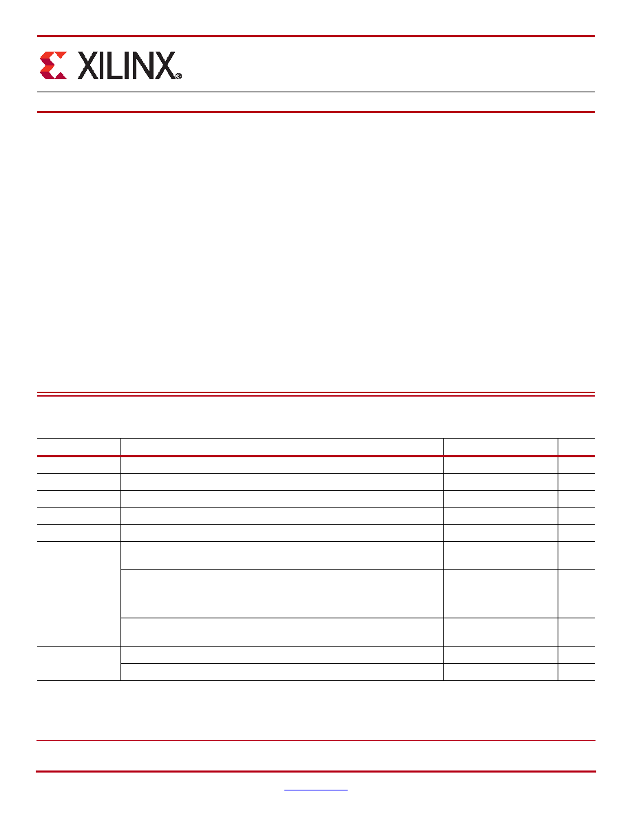
Table 1: Absolute Maximum Ratings
Symbol
Description
Units
VCCINT
Internal supply voltage relative to GND
–0.5 to 1.32
V
VCCAUX
Auxiliary supply voltage relative to GND
–0.5 to 3.0
V
VCCO
Output drivers supply voltage relative to GND
–0.5 to 3.75
V
VBATT
Key memory battery backup supply
–0.5 to 4.05
V
VREF
Input reference voltage
–0.3 to 3.75
V
VIN
I/O input voltage relative to GND
(all user and dedicated I/Os)
–0.75 to 4.05
V
I/O input voltage relative to GND
(restricted to maximum of 100 user I/Os)(3,4)
–0.95 to 4.4
(Commercial Temperature)
–0.85 to 4.3
(Industrial Temperature)
V
2.5V or below I/O input voltage relative to GND
(user and dedicated I/Os)
–0.75 to VCCO +0.5
V
IIN
Current applied to an I/O pin, powered or unpowered
±100
mA
Total current applied to all I/O pins, powered or unpowered
±200
mA
相關(guān)PDF資料 |
PDF描述 |
|---|---|
| XC4VFX100-11FFG1152I | FPGA, 10544 CLBS, 1181 MHz, PBGA1152 |
| XC4VFX100-11FFG1517I | FPGA, 10544 CLBS, 1181 MHz, PBGA1517 |
| XC4VFX100-12FFG1152C | FPGA, 10544 CLBS, 1181 MHz, PBGA1152 |
| XC4VFX100-12FFG1517C | FPGA, 10544 CLBS, 1181 MHz, PBGA1517 |
| XC5206-3PCG84I | FPGA, 196 CLBS, 6000 GATES, 83 MHz, PQCC84 |
相關(guān)代理商/技術(shù)參數(shù) |
參數(shù)描述 |
|---|---|
| XC4VFX100-11FF1152C | 制造商:Xilinx 功能描述:FPGA VIRTEX-4 94896 CELLS 90NM 1.2V 1152FCBGA - Trays |
| XC4VFX100-11FF1152CES1 | 制造商:Xilinx 功能描述: |
| XC4VFX100-11FF1152CES4 | 制造商:Xilinx 功能描述: |
| XC4VFX100-11FF1152CES4S | 制造商:Xilinx 功能描述: |
| XC4VFX100-11FF1152I | 功能描述:IC FPGA VIRTEX-4FX 1517FFBGA RoHS:否 類別:集成電路 (IC) >> 嵌入式 - FPGA(現(xiàn)場可編程門陣列) 系列:Virtex®-4 FX 產(chǎn)品變化通告:XC4000(E,L) Discontinuation 01/April/2002 標(biāo)準(zhǔn)包裝:24 系列:XC4000E/X LAB/CLB數(shù):100 邏輯元件/單元數(shù):238 RAM 位總計:3200 輸入/輸出數(shù):80 門數(shù):3000 電源電壓:4.5 V ~ 5.5 V 安裝類型:表面貼裝 工作溫度:-40°C ~ 100°C 封裝/外殼:120-BCBGA 供應(yīng)商設(shè)備封裝:120-CPGA(34.55x34.55) |
發(fā)布緊急采購,3分鐘左右您將得到回復(fù)。