- 您現(xiàn)在的位置:買賣IC網(wǎng) > PDF目錄371302 > X9430WS24-2.7 (INTERSIL CORP) Dual Digitally Controlled Potentiometer (XDCP) with Operational Amplifier PDF資料下載
參數(shù)資料
| 型號(hào): | X9430WS24-2.7 |
| 廠商: | INTERSIL CORP |
| 元件分類: | 數(shù)字電位計(jì) |
| 英文描述: | Dual Digitally Controlled Potentiometer (XDCP) with Operational Amplifier |
| 中文描述: | DUAL 10K DIGITAL POTENTIOMETER, 3-WIRE SERIAL CONTROL INTERFACE, 64 POSITIONS, PDSO24 |
| 封裝: | PLASTIC, SOIC-24 |
| 文件頁(yè)數(shù): | 5/21頁(yè) |
| 文件大?。?/td> | 881K |
| 代理商: | X9430WS24-2.7 |
第1頁(yè)第2頁(yè)第3頁(yè)第4頁(yè)當(dāng)前第5頁(yè)第6頁(yè)第7頁(yè)第8頁(yè)第9頁(yè)第10頁(yè)第11頁(yè)第12頁(yè)第13頁(yè)第14頁(yè)第15頁(yè)第16頁(yè)第17頁(yè)第18頁(yè)第19頁(yè)第20頁(yè)第21頁(yè)

X9430
– Preliminary Information
Characteristics subject to change without notice.
5 of 21
REV 1.0 6/20/00
www.xicor.com
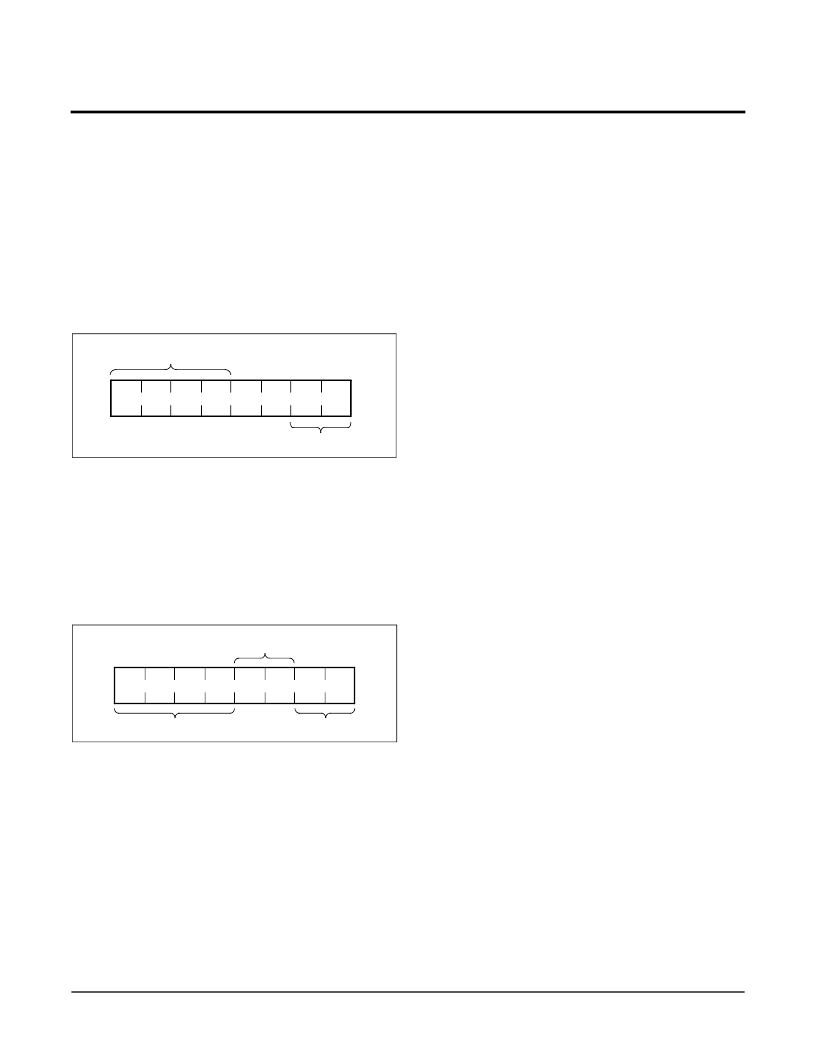
The two least significant bits in the ID byte select one of
four devices on the bus. The physical device address is
defined by the state of the A
0
-A
1
input pins. The X9430
compares the serial data stream with the address input
state; a successful compare of both address bits is
required for the X9430 to successfully continue the
command sequence. The A
0
–A
1
inputs can be actively
driven by CMOS input signals or tied to V
CC
or V
SS
.
The remaining two bits in the slave byte must be set to 0.
Figure 1. Identification Byte Format
Instruction Byte
The next byte sent to the X9430 contains the instruc-
tion and register pointer information. The four most sig-
nificant bits are the instruction. The next four bits point
to one of the WCRs of the two pots, and when applica-
ble, they point to one of four associated data registers.
The format is shown below in Figure 2.
Figure 2. Instruction Byte Format
The four high order bits of the instruction byte specify
the operation. The next two bits (R
1
and R
0
) select one
of the four registers that is to be acted upon when a
register oriented instruction is issued. The last bit (P
0
)
selects which one of the two potentiometers is to be
affected by the instruction.
Four of the ten instructions are two bytes in length and
end with the transmission of the instruction byte.
The basic sequence of the two byte instructions is illus-
trated in Figure 3. These two-byte instructions
exchange data between a wiper counter register and
one of the four data registers associated with each. A
transfer from a data register to a wiper counter register
is essentially a write to a static RAM. The response of
the wiper to this action will be delayed t
WRL
. A transfer
from the wiper counter register (current wiper position)
to a data register is a write to nonvolatile memory and
takes a minimum of t
WR
to complete. The transfer can
occur between one of the two potentiometers and one
of its associated registers; or it may occur globally,
wherein the transfer occurs between both of the poten-
tiometers and one of their associated registers.
Five instructions require a three-byte sequence to com-
plete. These instructions transfer data between the
host and the X9430; either between the host and one
of the data registers or directly between the host and
the Wiper Counter and Registers. These instructions
are: 1) Read Wiper Counter Register, read the current
wiper position of the selected pot 2) Write Wiper
Counter Register, i.e. change current wiper position of
the selected pot; 3) Read Data Register, read the con-
tents of the selected nonvolatile register; 4) Write Data
Register, write a new value to the selected data register;
5)Read Status, returns the contents of the WIP bit which
indicates if an internal write cycle is in progress.
The sequence of these operations is shown in Figure 4
and Figure 5.
The final command is Increment/Decrement. It is differ-
ent from the other commands, because it’s length is
indeterminate. Once the command is issued, the mas-
ter can clock the selected wiper up and/or down in one
resistor segment steps; thereby, providing a fine tuning
capability to the host. For each SCK clock pulse (t
HIGH
)
while SI is HIGH, the selected wiper will move one
resistor segment towards the V
H
terminal. Similarly, for
each SCK clock pulse while SI is LOW, the selected
wiper will move one resistor segment towards the V
L
terminal. A detailed illustration of the sequence and
timing for this operation are shown in Figure 6 and
Figure 7.
1
0
0
0
0
A1
A0
Device Type
Identifier
Device Address
1
I1
I2
I3
I0
R1
R0
0
P0
WCR Select
Register
Select
Instructions
相關(guān)PDF資料 |
PDF描述 |
|---|---|
| X9430WS24I | Dual Digitally Controlled Potentiometer (XDCP) with Operational Amplifier |
| X9430WV24I-2.7 | Dual Digitally Controlled Potentiometer (XDCP) with Operational Amplifier |
| X9440WP242.7 | Interface IC |
| X9440WP24I2.7 | Interface IC |
| X9440YP242.7 | Interface IC |
相關(guān)代理商/技術(shù)參數(shù) |
參數(shù)描述 |
|---|---|
| X9430WS24I | 功能描述:IC DUAL DCP +OPAMP 10K 64TP SO24 RoHS:否 類別:集成電路 (IC) >> 數(shù)據(jù)采集 - 數(shù)字電位器 系列:XDCP™ 產(chǎn)品培訓(xùn)模塊:Lead (SnPb) Finish for COTS Obsolescence Mitigation Program 標(biāo)準(zhǔn)包裝:1 系列:- 接片:256 電阻(歐姆):100k 電路數(shù):1 溫度系數(shù):標(biāo)準(zhǔn)值 35 ppm/°C 存儲(chǔ)器類型:非易失 接口:3 線串口 電源電壓:2.7 V ~ 5.25 V 工作溫度:-40°C ~ 85°C 安裝類型:表面貼裝 封裝/外殼:8-WDFN 裸露焊盤 供應(yīng)商設(shè)備封裝:8-TDFN-EP(3x3) 包裝:剪切帶 (CT) 產(chǎn)品目錄頁(yè)面:1399 (CN2011-ZH PDF) 其它名稱:MAX5423ETA+TCT |
| X9430WS24I-2.7 | 功能描述:IC DUAL DCP +OPAMP 10K 64TP SO24 RoHS:否 類別:集成電路 (IC) >> 數(shù)據(jù)采集 - 數(shù)字電位器 系列:XDCP™ 產(chǎn)品培訓(xùn)模塊:Lead (SnPb) Finish for COTS Obsolescence Mitigation Program 標(biāo)準(zhǔn)包裝:1 系列:- 接片:256 電阻(歐姆):100k 電路數(shù):1 溫度系數(shù):標(biāo)準(zhǔn)值 35 ppm/°C 存儲(chǔ)器類型:非易失 接口:3 線串口 電源電壓:2.7 V ~ 5.25 V 工作溫度:-40°C ~ 85°C 安裝類型:表面貼裝 封裝/外殼:8-WDFN 裸露焊盤 供應(yīng)商設(shè)備封裝:8-TDFN-EP(3x3) 包裝:剪切帶 (CT) 產(chǎn)品目錄頁(yè)面:1399 (CN2011-ZH PDF) 其它名稱:MAX5423ETA+TCT |
| X9430WS24M | 制造商:未知廠家 制造商全稱:未知廠家 功能描述:Interface IC |
| X9430WS24M2.7 | 制造商:未知廠家 制造商全稱:未知廠家 功能描述:Interface IC |
| X9430WV24 | 功能描述:IC DUAL DCP + OPAMP 10K 24TSSOP RoHS:否 類別:集成電路 (IC) >> 數(shù)據(jù)采集 - 數(shù)字電位器 系列:XDCP™ 產(chǎn)品培訓(xùn)模塊:Lead (SnPb) Finish for COTS Obsolescence Mitigation Program 標(biāo)準(zhǔn)包裝:1 系列:- 接片:256 電阻(歐姆):100k 電路數(shù):1 溫度系數(shù):標(biāo)準(zhǔn)值 35 ppm/°C 存儲(chǔ)器類型:非易失 接口:3 線串口 電源電壓:2.7 V ~ 5.25 V 工作溫度:-40°C ~ 85°C 安裝類型:表面貼裝 封裝/外殼:8-WDFN 裸露焊盤 供應(yīng)商設(shè)備封裝:8-TDFN-EP(3x3) 包裝:剪切帶 (CT) 產(chǎn)品目錄頁(yè)面:1399 (CN2011-ZH PDF) 其它名稱:MAX5423ETA+TCT |
發(fā)布緊急采購(gòu),3分鐘左右您將得到回復(fù)。