- 您現(xiàn)在的位置:買賣IC網(wǎng) > PDF目錄371269 > X68C75J Port Expander and E2 Memory PDF資料下載
參數(shù)資料
| 型號: | X68C75J |
| 英文描述: | Port Expander and E2 Memory |
| 中文描述: | 端口擴展和E2內(nèi)存 |
| 文件頁數(shù): | 12/26頁 |
| 文件大小: | 123K |
| 代理商: | X68C75J |
第1頁第2頁第3頁第4頁第5頁第6頁第7頁第8頁第9頁第10頁第11頁當(dāng)前第12頁第13頁第14頁第15頁第16頁第17頁第18頁第19頁第20頁第21頁第22頁第23頁第24頁第25頁第26頁

12
X68C75 SLIC
E
2
IRQ
The
IRQ
pin is an active LOW open-drain output. In
embedded systems applications, this signal is con-
nected to the microcontroller interrupt input pin through
either a direct connection or via an interrupt controller.
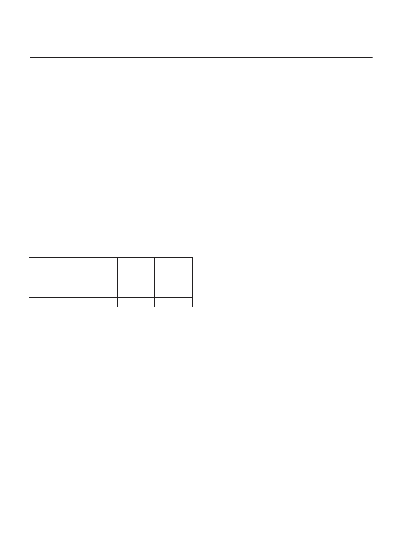
Table 1 depicts the three sources of interrupts and their
associated flags. Under normal conditions, the INT and
port interrupt flags are set, if the port which is configured
as an input has its strobe line toggled. If the port interrupt
enable flag is set, or gets set while the INT flag is set,
then the
IRQ
signal is asserted. The
IRQ
stays valid as
long as the interrupt flags are not cleared by the software
or the hardware.
Another interrupt source is the End Of Write flag (EOW)
which is set by the hardware at the end of every internal
programming cycle. The interrupt from this source is
controlled by the ENEE bit in ISR. If ENEE is enabled,
then EOW can generate an external interrupt. The
interrupt is cleared by setting EOW to “0”.
Table 1. X68C75 Interrupt Sources
Interrupt
Source
Interrupt
Enable
Status
Flag
INT
Flag
PORT A
PORT B
EOW
ENA
ENB
ENEE
INTA
INTB
EOW
“1”
“1”
—
2899 PGM T02.1
PORTS A & B INTERRUPTS
The X68C75 features two 8-bit I/O ports which are
equipped with a configurable interrupt module. The
interrupts are used to signal the reception of new data at
an input port data latch. When a port is configured as an
output, it can no longer generate any interrupts.
The input port interrupt mechanism is controlled by the
external strobe pins (STRA, STRB). Detecting a valid
transition on the pins will set the interrupt flags and latch
in the input data. The external interrupts from the ports
can be masked off using interrupt enable bits(ENA and
ENB) in ISR.
Once an external interrupt is asserted, clearing the
interrupt flags will cause the
IRQ
signal to return to its
idle state. There are two ways of resetting the interrupt
flags. The selection is made using the IRST bit in the
configuration register. If IRST is set, then the interrupt
flags are cleared by writing “0” to the bit positions
corresponding to the interrupt flags (INTA, INTB) in ISR.
When the IRST bit is cleared, reading the PDR automati-
cally clears the interrupt flags.
SOFTWARE CONTROLLED PORT OPERATIONS
The individual clock signals, that control the PDR input
latches and load the external data present on the port
pins, are generated by XORing the strobe polarity bit and
the strobe input of the port. The strobe polarity bits
(STPA, STPB) in CR can be used to program the active
edge of the strobe inputs. However, if the external strobe
input is permanently tied to V
SS
or V
CC
, then the strobe
polarity bit controls the PDR input latch clock signal.
When a port strobe and its polarity bit have identical logic
levels, the corresponding PDR latch is active and any
change in the port inputs will show up at the PDR latch
outputs. Holding the strobe input at current levels and
changing the strobe polarity bit value will generate a
positive transition on the PDR clock signal, causing the
latch outputs to reflect the previous logic state of the port
pins. The clock transition sets the interrupt flags, and if
the interrupts have been enabled, then an external
interrupt signal will be asserted.
This feature allows the port input operation by perma-
nently tying the STRx inputs to V
CC
or V
SS
, and using the
STPx bits in CR to control PDR latches. Another advan-
tage of this feature are software generated interrupts.
Since the clocking of the PDR latch causes the corre-
sponding port INTx flags to be set, by enabling the
interrupts the microcontroller is forced to execute the
interrupt service routine responsible to service the newly
latched data.
END OF WRITE (EOW) INTERRUPT
The internal programming cycle requires several milli-
seconds for either a single byte write or a page write. The
updated memory plane is inaccessible while the
programming is in progress. However, the opposite
plane is still available for program fetch and data read
operations.
The X68C75 has two means of signaling end of an
internal programming cycle. In the Toggle Bit Polling
technique, the last written byte is successively read. Bit
6 of read data toggles while the programming cycle is still
in progress. The software has to continually monitor
device responses and determine if it can again access
the plane.
In the other method, at the end of an internal program-
ming cycle, the hardware sets the EOW flag. The soft-
ware can either poll this flag or enable the interrupts by
setting the ENEE bit in ISR. Effective use of EOW is
made by clearing it prior to initiating a write operation. If
相關(guān)PDF資料 |
PDF描述 |
|---|---|
| X68C75JI | Port Expander and E2 Memory |
| X68C75JM | Port Expander and E2 Memory |
| X68C75L | Port Expander and E2 Memory |
| X68C75LI | Port Expander and E2 Memory |
| X68C75LM | Port Expander and E2 Memory |
相關(guān)代理商/技術(shù)參數(shù) |
參數(shù)描述 |
|---|---|
| X68C75JI | 制造商:XICOR 制造商全稱:Xicor Inc. 功能描述:Port Expander and E2 Memory |
| X68C75JM | 制造商:XICOR 制造商全稱:Xicor Inc. 功能描述:Port Expander and E2 Memory |
| X68C75L | 制造商:XICOR 制造商全稱:Xicor Inc. 功能描述:Port Expander and E2 Memory |
| X68C75LI | 制造商:XICOR 制造商全稱:Xicor Inc. 功能描述:Port Expander and E2 Memory |
| X68C75LM | 制造商:XICOR 制造商全稱:Xicor Inc. 功能描述:Port Expander and E2 Memory |
發(fā)布緊急采購,3分鐘左右您將得到回復(fù)。