- 您現(xiàn)在的位置:買賣IC網(wǎng) > PDF目錄371200 > X24256ZI-1.8 30V Single N-Channel HEXFET Power MOSFET in a D2-Pak package; A IRL7833S with Standard Packaging PDF資料下載
參數(shù)資料
| 型號: | X24256ZI-1.8 |
| 英文描述: | 30V Single N-Channel HEXFET Power MOSFET in a D2-Pak package; A IRL7833S with Standard Packaging |
| 中文描述: | EEPROM的 |
| 文件頁數(shù): | 2/18頁 |
| 文件大?。?/td> | 144K |
| 代理商: | X24256ZI-1.8 |

X24256
Characteristics subject to change without notice.
2 of 18
PIN DESCRIPTIONS
Serial Clock (SCL)
The SCL input is used to clock all data into and out of
the device.
Serial Data (SDA)
SDA is a bidirectional pin used to transfer data into
and out of the device. It is an open drain output and
may be wire-ORed with any number of open drain or
open collector outputs.
An open drain output requires the use of a pull-up
resistor. For selecting typical values, refer to the Pull-
up resistor selection graph at the end of this data
sheet.
Device Select (S
The device select inputs (S
the slave address. This allows up to four devices to
share a common bus. These inputs can be static or
actively driven. If used statically they must be tied to
V
SS
or V
CC
as appropriate. If actively driven, they
must be driven with CMOS levels (driven to V
V
SS
) and they must be constant between each start
and stop issued on the SDA bus. These pins have an
active pull down internally and will be sensed as low if
the pin is left unconnected.
0
, S
1
)
0
, S
1
) are used to set bits in
CC
or
Write Protect (WP)
WP must be constant between each start and stop
issued on the SDA bus and is always active (not
gated). The WP pin has an active pull down to disable
the write protection when the input is left floating. The
Write Protect input controls the Hardware Write Pro-
tect feature. When held LOW, Protection is disabled
and the device operates normally. When this input is
held HIGH, the device is protected, preventing
changes to any and all locations in the EEPROM array.
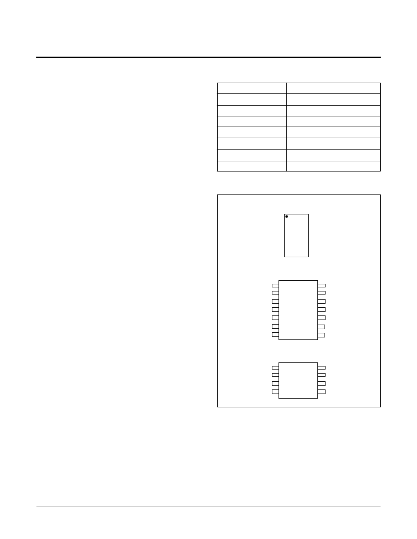
PIN NAMES
PIN CONFIGURATION
Symbol
S
0
, S
SDA
SCL
WP
V
SS
V
CC
NC
Description
1
Device Select Inputs
Serial Data
Serial Clock
Write Protect
Ground
Supply Voltage
No Connect
8 Lead PDIP/SOIC
VCC
WP
SCL
SDA
S0
S1
NC
1
2
3
4
6
5
7
8
X24256
VSS
14 Lead TSSOP
VCC
WP
NC
NC
SCL
SDA
S0
S1
NC
NC
NC
NC
1
2
3
4
5
7
6
X24256
VSS
NC
8
9
10
11
12
14
13
8-Lead XBGA: Top View
S
1
SDA
NC
SCL
VCC
VSS
S
0
WP
8
7
6
5
1
2
3
4
Powered by ICminer.com Electronic-Library Service CopyRight 2003
相關(guān)PDF資料 |
PDF描述 |
|---|---|
| X24256ZI-2.5 | EEPROM |
| X24320S8-1.8 | 16 Characters x 2 Lines, 5x7 Dot Matrix Character and Cursor |
| X24320S8-2.5 | 16 Characters x 2 Lines, 5x7 Dot Matrix Character and Cursor |
| X24320V14-2.5 | 400KHz 2-Wire Serial E2PROM with Block Lock |
| X24320 | 400KHz 2-Wire Serial E2PROM with Block Lock |
相關(guān)代理商/技術(shù)參數(shù) |
參數(shù)描述 |
|---|---|
| X24256ZI-2.5 | 制造商:未知廠家 制造商全稱:未知廠家 功能描述:EEPROM |
| X24257Z-2.5 | 制造商:XICOR 制造商全稱:Xicor Inc. 功能描述:400kHz 2-Wire Serial EEPROM with Block Lock |
| X242-883B | 制造商:未知廠家 制造商全稱:未知廠家 功能描述:X200 SERIES (CMOS) STANDARD SPECFITIONS |
| X242-SERIES | 制造商:未知廠家 制造商全稱:未知廠家 功能描述:Peripheral IC |
| X243 | 制造商:未知廠家 制造商全稱:未知廠家 功能描述:X200 SERIES (CMOS) STANDARD SPECFITIONS |
發(fā)布緊急采購,3分鐘左右您將得到回復(fù)。