- 您現(xiàn)在的位置:買(mǎi)賣(mài)IC網(wǎng) > PDF目錄372528 > X1242S8 200V Single N-Channel HEXFET Power MOSFET in a SO-8 package; A IRF7450 with Standard Packaging PDF資料下載
參數(shù)資料
| 型號(hào): | X1242S8 |
| 英文描述: | 200V Single N-Channel HEXFET Power MOSFET in a SO-8 package; A IRF7450 with Standard Packaging |
| 中文描述: | 集成電路表面貼裝與EEPROM的時(shí)鐘 |
| 文件頁(yè)數(shù): | 14/24頁(yè) |
| 文件大小: | 119K |
| 代理商: | X1242S8 |
第1頁(yè)第2頁(yè)第3頁(yè)第4頁(yè)第5頁(yè)第6頁(yè)第7頁(yè)第8頁(yè)第9頁(yè)第10頁(yè)第11頁(yè)第12頁(yè)第13頁(yè)當(dāng)前第14頁(yè)第15頁(yè)第16頁(yè)第17頁(yè)第18頁(yè)第19頁(yè)第20頁(yè)第21頁(yè)第22頁(yè)第23頁(yè)第24頁(yè)

X1242 – Preliminary Information
Characteristics subject to change without notice.
14 of 24
REV 1.1.3 10/15/00
www.xicor.com
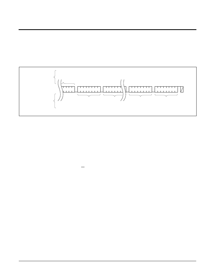
The data output is sequential, with the data from
address n followed by the data from address n + 1.
The address counter for read operations increments
through all page and column addresses, allowing the
entire memory contents to be serially read during one
operation. At the end of the address space the counter
“rolls over” to the start of the address space and the
X1242 continues to output data for each acknowledge
received. Refer to Figure 19 for the acknowledge and
data transfer sequence.
Figure 19. Sequential Read Sequence
Data
(2)
S
t
o
p
Slave
Address
Data
(n)
A
C
K
A
C
K
SDA Bus
Signals from
the Slave
Signals from
the Master
1
Data
(n-1)
A
C
K
A
C
K
(n is any integer greater than 1)
Data
(1)
DEVICE ADDRESSING
Following a start condition, the master must output a
Slave Address Byte. The first four bits of the Slave
Address Byte specify access to either the EEPROM
array or to the CCR. Slave bits ‘1010’ access the
EEPROM array. Slave bits ‘1101’ access the CCR.
Bit 3 through Bit 1 of the slave byte specify the device
select bits. These are set to ‘111’.
The last bit of the Slave Address Byte defines the
operation to be performed. When this R/W bit is a one,
then a read operation is selected. A zero selects a
write operation. Refer to Figure 19.
After loading the entire Slave Address Byte from the
SDA bus, the X1242 compares the device identifier
and device select bits with ‘1010111’ or ‘1101111’.
Upon a correct compare, the device outputs an
acknowledge on the SDA line.
Following the Slave Byte is a two byte word address.
The word address is either supplied by the master
device or obtained from an internal counter. On power
up the internal address counter is set to address 0h,
so a current address read of the EEPROM array starts
at address 0. When required, as part of a random
read, the master must supply the 2 Word Address
Bytes as shown in Figure 20.
In a random read operation, the slave byte in the
“dummy write” portion must match the slave byte in the
“read” section. That is if the random read is from the
array the slave byte must be 1010111x in both
instances. Similarly, for a random read of the Clock/
Control Registers, the slave byte must be 1101111x in
both places.
相關(guān)PDF資料 |
PDF描述 |
|---|---|
| X1242 | Real Time Clock/Calendar/Alarms/CPU Supervisor(實(shí)時(shí)時(shí)鐘/日歷/鬧鐘/帶EEPROM的監(jiān)控) |
| x1243(中文) | Real Time Clock/Calendar/Alarm with EEPROM(帶EEPROM的實(shí)時(shí)時(shí)鐘/日歷/鬧鐘) |
| X12xx-EVM(中文) | Xicor RTC X12xx-EVM User Guide(XICOR RTC X12xx-EVM評(píng)估板使用說(shuō)明) |
| X187 | TEMPERATURSICHERUNG 187GRAD 5ST |
| X25 | 40V Single N-Channel HEXFET Power MOSFET in a D2-Pak package; A IRL1004S with Standard Packaging |
相關(guān)代理商/技術(shù)參數(shù) |
參數(shù)描述 |
|---|---|
| X1243 | 制造商:INTERSIL 制造商全稱(chēng):Intersil Corporation 功能描述:Real Time Clock/Calendar/Alarm with EEPROM |
| X1243S8 | 制造商:XICOR 制造商全稱(chēng):Xicor Inc. 功能描述:Real Time Clock/Calendar/Alarm with EEPROM |
| X1243S8I | 制造商:Intersil Corporation 功能描述: 制造商:XICOR 功能描述: |
| X1243V8 | 制造商:XICOR 制造商全稱(chēng):Xicor Inc. 功能描述:Real Time Clock/Calendar/Alarm with EEPROM |
| X-1244 | 制造商:Pulse 功能描述:TRANSFORMERS - Rail/Tube |
發(fā)布緊急采購(gòu),3分鐘左右您將得到回復(fù)。