- 您現(xiàn)在的位置:買賣IC網(wǎng) > PDF目錄372526 > X1205V8Z (INTERSIL CORP) 2-Wire RTC Real Time Clock/Calendar PDF資料下載
參數(shù)資料
| 型號: | X1205V8Z |
| 廠商: | INTERSIL CORP |
| 元件分類: | XO, clock |
| 英文描述: | 2-Wire RTC Real Time Clock/Calendar |
| 中文描述: | REAL TIME CLOCK, PDSO8 |
| 封裝: | 4.40 MM, ROHS COMPLIANT, PLASTIC, TSSOP-8 |
| 文件頁數(shù): | 2/22頁 |
| 文件大小: | 407K |
| 代理商: | X1205V8Z |

X1205 – Preliminary Information
REV 1.0.9 8/29/02
Characteristics subject to change without notice.
2 of 22
www.xicor.com
DESCRIPTION
The powerful Dual Alarms can be set to any Clock/
Calendar value for a match. For instance, every
minute, every Tuesday, or 5:23 AM on March 21. The
alarms can be polled in the Status Register or provide
a hardware interrupt (IRQ Pin). There is a repeat
mode for the alarms allowing a periodic interrupt.
(continued)
The device offers a backup power input pin. This
V
BACK
pin allows the device to be backed up by battery
or SuperCap. The entire X1205 device is fully
operational from 2.7 to 5.5 volts and the clock/calendar
portion of the X1205 device remains fully operational
down to 1.8 volts (Standby Mode).
PIN DESCRIPTIONS
Serial Clock (SCL)
The SCL input is used to clock all data into and out of
the device. The input buffer on this pin is always active
(not gated).
Serial Data (SDA)
SDA is a bidirectional pin used to transfer data into and
out of the device. It has an open drain output and may
be wire ORed with other open drain or open collector
outputs. The input buffer is always active (not gated).
An open drain output requires the use of a pull-up
resistor. The output circuitry controls the fall time of the
output signal with the use of a slope controlled pull-
down. The circuit is designed for 400kHz 2-wire inter-
face speeds.
V
This input provides a backup supply voltage to the
device. V
BACK
supplies power to the device in the
event the V
CC
supply fails. This pin can be connected
to a battery, a Supercap or tied to ground if not used.
BACK
Interrupt Output – IRQ
This is an interrupt signal output. This signal notifies a
host processor that an alarm has occurred and
requests action. It is an open drain active low output.
X1, X2
The X1 and X2 pins are the input and output,
respectively, of an inverting amplifier. An external
32.768kHz quartz crystal is used with the X1205 to
supply a timebase for the real time clock. The
recommended crystal is a Citizen CFS206-32.768KDZF.
Internal compensation circuitry is included to form a
complete oscillator circuit. Care should be taken in the
placement of the crystal and the layout of the circuit.
Plenty of ground plane around the device and short
traces to X1 and X2 are highly recommended. See
Application section for more recommendations.
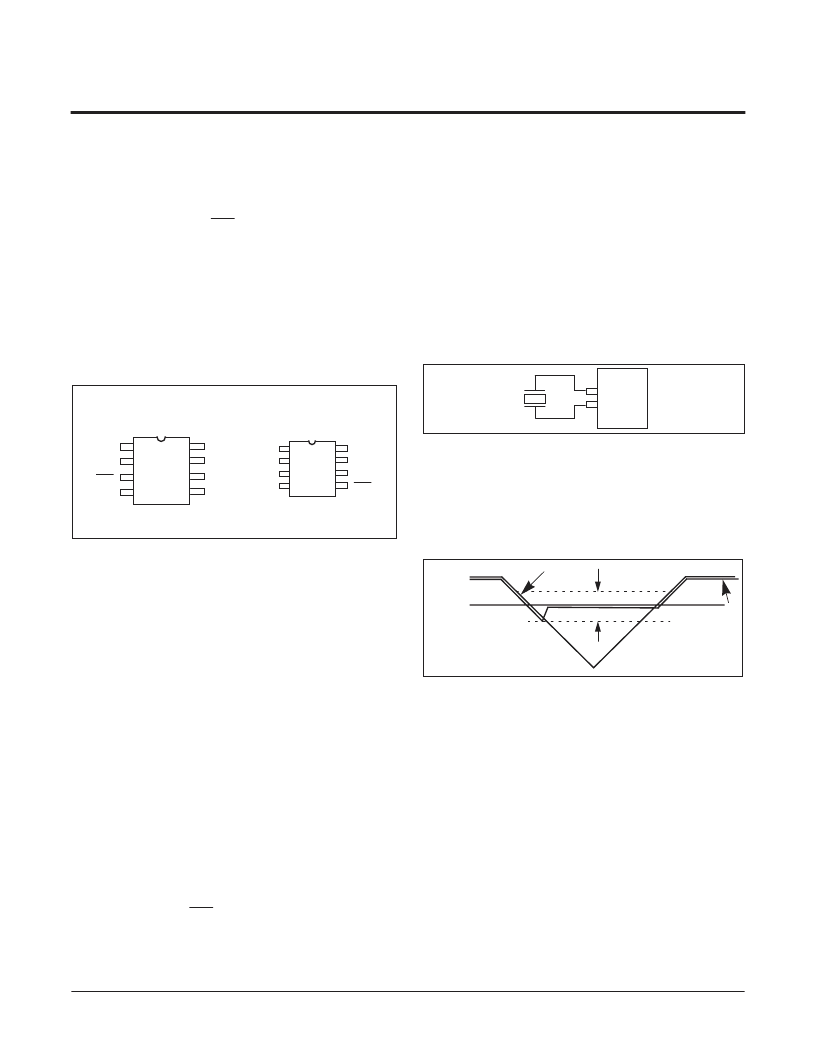
Figure 1. Recommended Crystal connection
POWER CONTROL OPERATION
The power control circuit accepts a V
input. The power control circuit powers the clock from
V
BACK
when V
CC
< V
BACK
- 0.2V. It will switch back to
power the device from V
CC
when V
Figure 2. Power Control
CC
and a V
BACK
CC
exceeds V
BACK
.
REAL TIME CLOCK OPERATION
The Real Time Clock (RTC) uses an external
32.768kHz quartz crystal to maintain an accurate inter-
nal representation of second, minute, hour, day, date,
month, and year. The RTC has leap-year correction.
The clock also corrects for months having fewer than
31 days and has a bit that controls 24 hour or AM/PM
format. When the X1205 powers up after the loss of
both V
CC
and V
BACK
, the clock will not operate until at
least one byte is written to the clock register.
Reading the Real Time Clock
The RTC is read by initiating a Read command and
specifying the address corresponding to the register of
the Real Time Clock. The RTC Registers can then be
read in a Sequential Read Mode. Since the clock runs
continuously and a read takes a finite amount of time,
there is the possibility that the clock could change during
NC = No internal connection
X2
V
BACK
V
CC
IRQ
SCL
SDA
V
SS
1
2
3
4
7
6
5
8
8-Pin TSSOP
X1205
X1
X2
V
BACK
SCL
SDA
V
CC
IRQ
V
SS
1
2
3
4
7
6
5
8
8-Pin SOIC
X1
X2
V
BACK
In
Voltage
V
CC
On
Off
相關(guān)PDF資料 |
PDF描述 |
|---|---|
| X1205V8ZT1 | 2-Wire RTC Real Time Clock/Calendar |
| X1205 | 2-Wire RTC Real Time Clock/Calendar |
| X1205S8 | 2-Wire RTC Real Time Clock/Calendar |
| X1205S8I | 2-Wire RTC Real Time Clock/Calendar |
| X1205S8IT1 | 2-Wire RTC Real Time Clock/Calendar |
相關(guān)代理商/技術(shù)參數(shù) |
參數(shù)描述 |
|---|---|
| X1205V8ZT1 | 制造商:INTERSIL 制造商全稱:Intersil Corporation 功能描述:2-Wire RTC Real Time Clock/Calendar |
| X1210MKX7R8BB564 | 制造商:Yageo / Phycomp 功能描述:0.56uF 25V SM CAP-X2Y FILTER 1210 X7R 20% Ni Barr w/100% Tin - free partial T/R at 500. |
| X121198-ISD | 制造商:Honeywell Sensing and Control 功能描述:RESISTIVE & OPTICAL |
| X-1214-1 | 制造商:Pulse Electronics Corporation 功能描述:DATA BUS - Rail/Tube |
| X-1215-1 | 制造商:Pulse Electronics Corporation 功能描述:DATA BUS - Rail/Tube |
發(fā)布緊急采購,3分鐘左右您將得到回復。