- 您現(xiàn)在的位置:買賣IC網(wǎng) > PDF目錄62818 > WV3EG265M64EFSU262D4-S (WHITE ELECTRONIC DESIGNS CORP) 128M X 64 DDR DRAM MODULE, 0.75 ns, DMA200 PDF資料下載
參數(shù)資料
| 型號(hào): | WV3EG265M64EFSU262D4-S |
| 廠商: | WHITE ELECTRONIC DESIGNS CORP |
| 元件分類: | DRAM |
| 英文描述: | 128M X 64 DDR DRAM MODULE, 0.75 ns, DMA200 |
| 封裝: | SODIMM-200 |
| 文件頁(yè)數(shù): | 5/10頁(yè) |
| 文件大?。?/td> | 148K |
| 代理商: | WV3EG265M64EFSU262D4-S |
4
White Electronic Designs Corporation (602) 437-1520 www.wedc.com
White Electronic Designs WV3EG265M64EFSU-D4
October 2005
Rev. 1
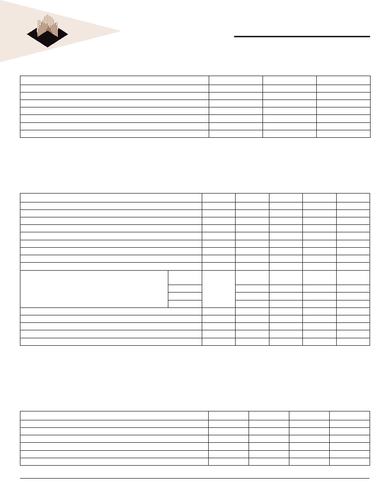
ABSOLUTE MAXIMUM RATINGS
Parameter
Symbol
Value
Units
Voltage on any pin relative to VSS
VIN, VOUT
-0.5 to 3.3
V
Voltage on VCC supply relative to VSS
VCC
-1.0 to 3.6
V
Voltage on VCCQ supply relative to VSS
VCCQ
-1.0 to 3.6
V
Storage Temperature
TSTG
-55 to +150
°C
Operating Temperature
TA
0 to +70
°C
Power Dissipation
PD
16
W
Short Circuit Current
IOS
50
mA
Note:
Permanent device damage may occur if ABSOLUTE MAXIMUM RATINGS are exceeded.
Functional operation should be restricted to recommended operating condition.
Exposure to higher than recommended voltage for extended periods of time could affect device reliability.
DC CHARACTERISTICS
0°C
≤ TA ≤ 70°C, VCC = 2.5V ± 0.2V
Parameter
Symbol
Min
Max
Unit
Note
Supply voltage DDR266/DDR333 (nominal VCC of 2.5V)
VCC
2.3
2.7
I/O Supply voltage DDR266/DDR333 (nominal VCC of 2.5V)
VCCQ
2.3
2.7
V
I/O Reference voltage
VREF
0.49*VCCQ
0.51*VCCQ
V1
I/O Termination voltage
VTT
VREF-0.04
VREF+0.04
V
2
Input logic high voltage
VIH(DC)
VREF+0.15
VCCQ+0.30
V
Input logic low voltage
VIL(DC)
-0.3
VREF-0.15
V
Input voltage level, CK and CK#
VIN(DC)
-0.3
VCCQ+0.30
V
Input differential voltage, CK and CK#
VID(DC)
0.3
VCCQ+0.60
V
3
Input crossing point voltage, CK and CK#
VIX(DC)
0.3
VCCQ+0.60
V
Input leakage current
Addr, CAS#,
RAS#, WE#
II
-32
32
uA
CS#, CKE
-16
16
uA
CK, CK#
-10
uA
DM
-4
4
uA
Output leakage current
IOZ
-10
10
uA
Output high current (normal strengh); VOUT = V +0.84V
IOH
-16.8
—
mA
Output high current (normal strengh); VOUT = VTT -0.84V
IOL
16.8
—
mA
Output high current (half strengh); VOUT = VTT +0.45V
IOH
-9
—
mA
Output high current (half strengh); VOUT = VTT -0.45V
IOL
9—
mA
NOTES:
1. VREF is expected to be equal to 0.5*VCCQ of the transmitting device, and to track variations in the DC level of the same. Peak to peak noise on VREF may not exceed ±2% of the DC
value
2. VTT is not applied directly to the device. VTT is a system supply for signal termination resistors, is expected to be set equal to VREF, and must track variations in the DC level of VREF
3. VID is the magnitude of the difference between the input level on CK and the input level on CK#.
CAPACITANCE
VCC = 2.5V, VCCQ = 2.5V, TA = 25°C, f = 1MHz
Parameter
Symbol
Min
Max
Unit
Input Capacitance (A0-A12, BA0-BA1, RAS#, CAS#, WE#)
CIN1
28
44
pF
Input Capacitance (CKE0, CKE1)
CIN2
16
24
pF
Input Capacitance (CS0#, CS1#)
CIN3
16
24
pF
Input Capacitance (CLK0, CLK0#)
CIN4
6
7.5
pF
Input Capacitance (DM0-DM7)
CIN5
11
13
pF
Data and DQS input/output capacitance (DQ0-DQ63)
COUT1
11
13
pF
相關(guān)PDF資料 |
PDF描述 |
|---|---|
| WV3EG6434S335BD4S | 32M X 64 DDR DRAM MODULE, 0.7 ns, DMA200 |
| WWB201ES40 | 1M X 16 MULTI DEVICE SRAM CARD, 200 ns, XMA68 |
| WWB513ES40 | 256K X 16 MULTI DEVICE SRAM CARD, 200 ns, XMA68 |
| ##PCFMJ-001 | 0.45 MHz, CERAMIC BPF |
| ##PCFMT-023 | 0.45 MHz, CERAMIC BRF |
相關(guān)代理商/技術(shù)參數(shù) |
參數(shù)描述 |
|---|---|
| WV3EG265M64EFSU-D4 | 制造商:WEDC 制造商全稱:White Electronic Designs Corporation 功能描述:1GB- 2x64Mx64 DDR SDRAM UNBUFFERED, w/PLL |
| WV3EG265M72EFSU262D4IM | 制造商:WEDC 制造商全稱:White Electronic Designs Corporation 功能描述:1GB - 2x64Mx72 DDR SDRAM, UNBUFFERED, PLL, FBGA |
| WV3EG265M72EFSU262D4IMG | 制造商:WEDC 制造商全稱:White Electronic Designs Corporation 功能描述:1GB - 2x64Mx72 DDR SDRAM, UNBUFFERED, PLL, FBGA |
| WV3EG265M72EFSU262D4IN | 制造商:WEDC 制造商全稱:White Electronic Designs Corporation 功能描述:1GB - 2x64Mx72 DDR SDRAM, UNBUFFERED, PLL, FBGA |
| WV3EG265M72EFSU262D4ING | 制造商:WEDC 制造商全稱:White Electronic Designs Corporation 功能描述:1GB - 2x64Mx72 DDR SDRAM, UNBUFFERED, PLL, FBGA |
發(fā)布緊急采購(gòu),3分鐘左右您將得到回復(fù)。