- 您現(xiàn)在的位置:買賣IC網(wǎng) > PDF目錄361926 > WS1M32-17G3X 1Mx32 SRAM Module(1Mx32靜態(tài)RAM模塊(存取時間17ns)) PDF資料下載
參數(shù)資料
| 型號: | WS1M32-17G3X |
| 英文描述: | 1Mx32 SRAM Module(1Mx32靜態(tài)RAM模塊(存取時間17ns)) |
| 中文描述: | 1Mx32的SRAM模塊(1Mx32靜態(tài)內(nèi)存模塊(存取時間17ns)) |
| 文件頁數(shù): | 3/6頁 |
| 文件大?。?/td> | 150K |
| 代理商: | WS1M32-17G3X |
White Microelectronics Phoenix, AZ (602) 437-1520
4
S
3
Parameter
Symbol
-17
-20
-25
Units
Read Cycle
Min
Max
Min
Max
Min
Max
Read Cycle Time
t
RC
17
20
25
ns
Address Access Time
t
AA
17
20
25
ns
Output Hold from Address Change
t
OH
0
0
0
ns
Chip Select Access Time
t
ACS
17
20
25
ns
Output Enable to Output Valid
t
OE
10
10
12
ns
Chip Select to Output in Low Z
t
CLZ
1
2
2
2
ns
Output Enable to Output in Low Z
t
OLZ
1
0
0
0
ns
Chip Disable to Output in High Z
t
CHZ
1
12
12
12
ns
Output Disable to Output in High Z
t
OHZ
1
12
12
12
ns
1. This parameter is guaranteed by design but not tested.
AC CHARACTERISTICS
(V
CC
= 5.0V, GND = 0V, T
A
= -55
°
C to +125
°
C)
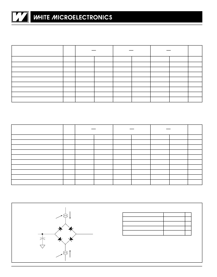
AC TEST CIRCUIT
NOTES:
V
Z
is programmable from -2V to +7V.
I
OL
& I
OH
programmable from 0 to 16mA.
Tester Impedance Z
0
= 75
.
V
Z
is typically the midpoint of V
OH
and V
OL
.
I
OL
& I
OH
are adjusted to simulate a typical resistive load circuit.
ATE tester includes jig capacitance.
I
Current Source
D.U.T.
C = 50 pf
I
OL
V
≈
1.5V
(Bipolar Supply)
Z
Current Source
OH
AC CHARACTERISTICS
(V
CC
= 5.0V, GND = 0V, T
A
= -55
°
C to +125
°
C)
AC TEST CONDITIONS
Parameter
Input Pulse Levels
Input Rise and Fall
Input and Output Reference Level
Output Timing Reference Level
Typ
Unit
V
ns
V
V
V
IL
= 0, V
IH
= 3.0
5
1.5
1.5
Parameter
Symbol
-17
-20
-25
Units
Write Cycle
Min
Max
Min
Max
Min
Max
Write Cycle Time
t
WC
17
20
25
ns
Chip Select to End of Write
t
CW
15
15
17
ns
Address Valid to End of Write
t
AW
15
15
17
ns
Data Valid to End of Write
t
DW
11
12
13
ns
Write Pulse Width
t
WP
15
15
17
ns
Address Setup Time
t
AS
2
2
2
ns
Address Hold Time
t
AH
0
0
0
ns
Output Active from End of Write
t
OW
1
2
3
4
ns
Write Enable to Output in High Z
t
WHZ
1
9
11
13
ns
Data Hold Time
t
DH
0
0
0
ns
1. This parameter is guaranteed by design but not tested.
WS1M32-XG3X
相關(guān)PDF資料 |
PDF描述 |
|---|---|
| WS1M32-20G3X | 1Mx32 SRAM Module(1Mx32靜態(tài)RAM模塊(存取時間20ns)) |
| WS1M32-G3C | 1Mx32 SRAM MODULE |
| WS1M32-G3CA | 1Mx32 SRAM MODULE |
| WS1M32-G3I | 1Mx32 SRAM MODULE |
| WS1M32-G3IA | 1Mx32 SRAM MODULE |
相關(guān)代理商/技術(shù)參數(shù) |
參數(shù)描述 |
|---|---|
| WS1M32-17G4TI | 制造商:未知廠家 制造商全稱:未知廠家 功能描述:x32 SRAM Module |
| WS1M32-17G4TM | 制造商:未知廠家 制造商全稱:未知廠家 功能描述:x32 SRAM Module |
| WS1M32-17HSC | 制造商:未知廠家 制造商全稱:未知廠家 功能描述:1Mx32 SRAM MODULE |
| WS1M32-17HSCA | 制造商:未知廠家 制造商全稱:未知廠家 功能描述:1Mx32 SRAM MODULE |
| WS1M32-17HSI | 制造商:未知廠家 制造商全稱:未知廠家 功能描述:1Mx32 SRAM MODULE |
發(fā)布緊急采購,3分鐘左右您將得到回復(fù)。