- 您現(xiàn)在的位置:買(mǎi)賣(mài)IC網(wǎng) > PDF目錄361880 > WM2627 (Wolfson Microelectronics) Quad 8-Bit Serial Input Voltage Output DAC PDF資料下載
參數(shù)資料
| 型號(hào): | WM2627 |
| 廠商: | Wolfson Microelectronics |
| 英文描述: | Quad 8-Bit Serial Input Voltage Output DAC |
| 中文描述: | 四8位串行輸入電壓輸出DAC |
| 文件頁(yè)數(shù): | 9/11頁(yè) |
| 文件大小: | 107K |
| 代理商: | WM2627 |
WM2627
Production Data
WOLFSON MICROELECTRONICS LTD
PD Rev 1.0 April 2001
9
SERIAL INTERFACE
To start transferring data, the device first has to be enabled with NCS set to low. Then, a falling edge
of FS starts shifting the data bit-per-bit (starting with the MSB) to the internal register on the falling
edges of SCLK. After 16 bits have been transferred, the next rising edge on SCLK or FS causes the
content of the shift register to be moved to the DAC holding latch. If NLDAC is low, the DAC latch will
also be updated immediately.
The serial interface of the device can be used in two basic modes:
four wire (with chip select)
three wire (without chip select)
Using chip select (four wire mode), it is possible to have more than one device connected to the serial
port of the data source (DSP or microcontroller). If there is no need to have more than one device on
the serial bus, then NCS can be tied low.
SERIAL CLOCK AND UPDATE RATE
Figure 1 shows the device timing. The maximum serial rate is:
f
SCLK
max =
MHz
20
t
t
1
+
min
WCL
min
WCH
=
The digital update rate is limited to an 800ns period, or 1.25MHz frequency. However, the DAC
settling time to 8 bits limits the update rate for large input step transitions.
SOFTWARE CONFIGURATION OPTIONS
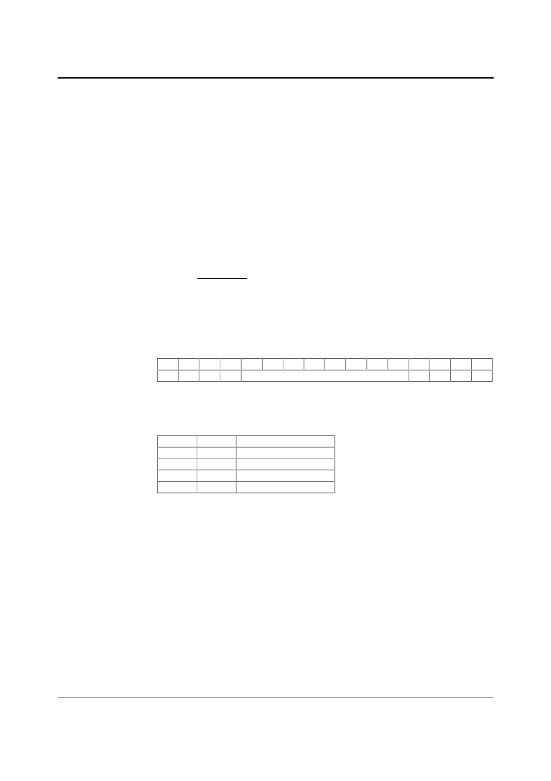
The 16 bits of data can be transferred with the sequence shown in Table 2. D11-D2 contains the
8-bit data word. D15-D12 hold the programmable options.
D15
A1
Table 2 Register Map
D14
A0
D13
PWR SPD
D12
D11
D10
D9
New DAC value (8 bits)
D8
D7
D6
D5
D4
D3
0
D2
0
D1
0
D0
0
DAC ADDRESSING
A particular DAC (A, B, C, D) within the device is selected by A1 and A0 within the input word.
A1
0
0
1
1
A0
0
1
0
1
DAC ADDRESS
DAC A
DAC B
DAC C
DAC D
PROGRAMMABLE SETTLING TIME (SPD – BIT D12)
Settling time is a software selectable 2.5
μ
s or 8.5
μ
s, typical to within
±
0.1LSB of final value. This is
controlled by the value of SPD
–
Bit D12 and an associated DAC address. A ONE defines a settling
time of 2.5
μ
s, a ZERO defines a settling time of 8.5
μ
s for that DAC.
PROGRAMMABLE POWER DOWN
The power down function is controlled by PWR - Bit D13 and an associated DAC address. A ZERO
configures that DAC as active, a ONE configures that DAC into power down mode.
相關(guān)PDF資料 |
PDF描述 |
|---|---|
| WM2627IDT | Quad 8-Bit Serial Input Voltage Output DAC |
| WM2629 | Octal 8-bit, Serial Input, Voltage Output DAC with Power Down |
| WM2630CDT | Octal 12-bit, Serial Input, Voltage Output DAC with Internal Reference |
| WM2630 | Octal 12-bit, Serial Input, Voltage Output DAC with Internal Reference |
| WM2630IDT | Octal 12-bit, Serial Input, Voltage Output DAC with Internal Reference |
相關(guān)代理商/技術(shù)參數(shù) |
參數(shù)描述 |
|---|---|
| WM2627CDT | 制造商:WOLFSON 制造商全稱(chēng):WOLFSON 功能描述:Quad 8-Bit Serial Input Voltage Output DAC |
| WM2627IDT | 制造商:WOLFSON 制造商全稱(chēng):WOLFSON 功能描述:Quad 8-Bit Serial Input Voltage Output DAC |
| WM2629 | 制造商:WOLFSON 制造商全稱(chēng):WOLFSON 功能描述:Octal 8-bit, Serial Input, Voltage Output DAC with Power Down |
| WM2630 | 制造商:WOLFSON 制造商全稱(chēng):WOLFSON 功能描述:Octal 12-bit, Serial Input, Voltage Output DAC with Internal Reference |
| WM2630CDT | 制造商:WOLFSON 制造商全稱(chēng):WOLFSON 功能描述:Octal 12-bit, Serial Input, Voltage Output DAC with Internal Reference |
發(fā)布緊急采購(gòu),3分鐘左右您將得到回復(fù)。