- 您現(xiàn)在的位置:買賣IC網(wǎng) > PDF目錄361880 > WM2627IDT (Wolfson Microelectronics) Quad 8-Bit Serial Input Voltage Output DAC PDF資料下載
參數(shù)資料
| 型號(hào): | WM2627IDT |
| 廠商: | Wolfson Microelectronics |
| 英文描述: | Quad 8-Bit Serial Input Voltage Output DAC |
| 中文描述: | 四8位串行輸入電壓輸出DAC |
| 文件頁數(shù): | 1/11頁 |
| 文件大小: | 107K |
| 代理商: | WM2627IDT |
WM2627
Quad 8-Bit Serial Input Voltage Output DAC
Production Data, April 2001, Rev 1.0
WOLFSON MICROELECTRONICS LTD
Lutton Court, Bernard Terrace, Edinburgh, EH8 9NX, UK
Tel: +44 (0) 131 667 9386
Fax: +44 (0) 131 667 5176
Email: sales@wolfson.co.uk
www.wolfsonmicro.com
Production Data
Datasheets
contain final
specifications current on publication date.
Supply of products conforms to Wolfson
Microelectronics’ Terms and Conditions.
2001 Wolfson Microelectronics Ltd
.
FEATURES
Four 8-bit voltage output DACs
Dual 2.7V to 5.5V supply (separate digital and analogue
supplies)
DNL
±
0.03 LSB, INL
±
0.3 LSB typical
Low power consumption:
-
3mW, slow mode - 3V supply
-
9mW, fast mode - 3V supply
DSP and microprocessor compatible serial interface
Programmable settling time of 2.5
μ
s or 8.5
μ
s typical
APPLICATIONS
Battery powered test instruments
Digital offset and gain adjustment
Battery operated/remote industrial controls
Machine and motion control devices
Wireless telephone and communication systems
Arbitrary waveform generation
Robotics
ORDERING INFORMATION
DEVICE
TEMP. RANGE
PACKAGE
WM2627CDT
0
°
to 70
°
C
16-pin TSSOP
WM2627IDT
-40
°
to 85
°
C
16-pin TSSOP
DESCRIPTION
The WM2627 is a quadruple 8-bit voltage output, resistor string,
digital-to-analogue converter. Each DAC can be individually
powered down under software control. A hardware controlled
mode is provided that powers down all DACs. Power down
reduces current consumption to 1
μ
A.
The device has been designed to interface efficiently to industry
standard microprocessors and DSPs. It is programmed with a
16-bit serial word comprising of a DAC address, individual DAC
control bits and an 8-bit value.
The WM2627 has provision for two supplies: one supply for the
serial interface (DVDD, DGND), and one for the DACs,
reference buffers and output buffers (AVDD, AGND). This
enables a typical application where the device can be controlled
via a microprocessor operating on a 3V supply, with the DACs
operating on a 5V supply. Alternatively, the supplies can be tied
together in a single supply application.
Excellent performance is delivered with a typical DNL of
±
0.03
LSB. The settling time of the DAC is programmable to allow the
designer to optimize speed versus power dissipation. The
output stage is buffered by a x2 gain near rail-to-rail amplifier,
which features a Class AB output stage. DACs A and B can
have a different reference voltage to DACs C and D.
The device is available in a 16-pin TSSOP package.
Commercial
temperature
(0
°
temperature (-40
°
to 85
°
C) variants are supported.
to
70
°
C)
and
Industrial
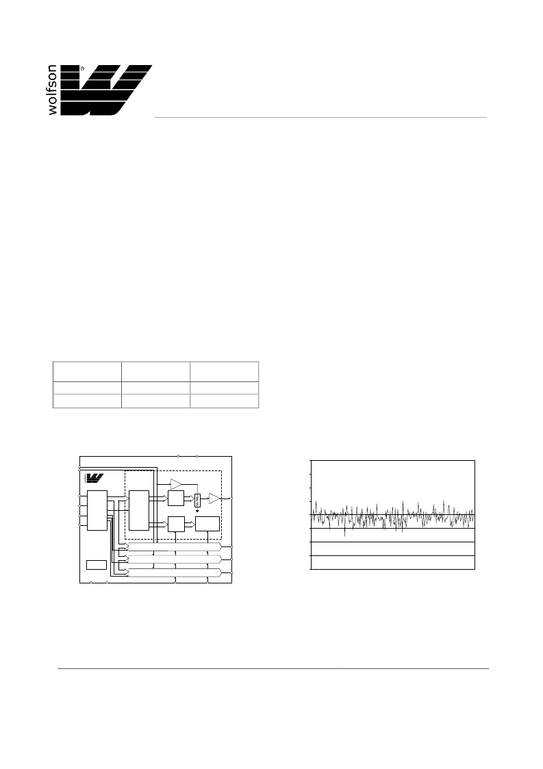
BLOCK DIAGRAM
TYPICAL PERFORMANCE
(11) OUTD
(12) OUTC
(13) OUTB
(14) OUTA
10-BIT
DATA AND
CONTROL
HOLDING
LATCH
8-BIT
DAC
LATCH
16-BIT
SHIFT
REGISTER
AND
CONTROL
LOGIC
REFINAB (15)
REFINCD (10)
POWER-ON
RESET
DIN (4)
FS (7)
SCLK (5)
NCS (6)
(9)
AGND
(8)
DGND
(3)
NLDAC
(2)
NPD
AVDD
(16)
DVDD
(1)
X2
DAC A
DAC C
DAC D
POWERDOWN/
SPEED
CONTROL
WM2627
2-BIT
CONTROL
LATCH
DAC B
X1
DAC
OUTPUT
BUFFER
data
REFERENCE
INPUT BUFFER
AVDD = DVDD = 5V, VREF = 2.048V, Slow Mode
-0.04
-0.03
-0.02
-0.01
0
0.01
0.02
0.03
0.04
0
32
64
96
128
160
192
224
256
DIGITAL CODE
D
相關(guān)PDF資料 |
PDF描述 |
|---|---|
| WM2629 | Octal 8-bit, Serial Input, Voltage Output DAC with Power Down |
| WM2630CDT | Octal 12-bit, Serial Input, Voltage Output DAC with Internal Reference |
| WM2630 | Octal 12-bit, Serial Input, Voltage Output DAC with Internal Reference |
| WM2630IDT | Octal 12-bit, Serial Input, Voltage Output DAC with Internal Reference |
| WM2633 | BOX 6.88X4.88X1.51 9V GRY |
相關(guān)代理商/技術(shù)參數(shù) |
參數(shù)描述 |
|---|---|
| WM2629 | 制造商:WOLFSON 制造商全稱:WOLFSON 功能描述:Octal 8-bit, Serial Input, Voltage Output DAC with Power Down |
| WM2630 | 制造商:WOLFSON 制造商全稱:WOLFSON 功能描述:Octal 12-bit, Serial Input, Voltage Output DAC with Internal Reference |
| WM2630CDT | 制造商:WOLFSON 制造商全稱:WOLFSON 功能描述:Octal 12-bit, Serial Input, Voltage Output DAC with Internal Reference |
| WM2630IDT | 制造商:Rochester Electronics LLC 功能描述:- Bulk |
| WM2631 | 制造商:WOLFSON 制造商全稱:WOLFSON 功能描述:Octal 10-bit, Serial Input, Voltage Output DAC with Internal Reference |
發(fā)布緊急采購,3分鐘左右您將得到回復(fù)。