- 您現(xiàn)在的位置:買賣IC網(wǎng) > PDF目錄361880 > WM2626ID (Wolfson Microelectronics) Low Power Dual 8-bit Serial Input DAC with Internal Reference PDF資料下載
參數(shù)資料
| 型號: | WM2626ID |
| 廠商: | Wolfson Microelectronics |
| 英文描述: | Low Power Dual 8-bit Serial Input DAC with Internal Reference |
| 中文描述: | 低功耗雙8位串行輸入DAC的內(nèi)部參考 |
| 文件頁數(shù): | 4/11頁 |
| 文件大小: | 109K |
| 代理商: | WM2626ID |
WM2626
Production Data
WOLFSON MICROELECTRONICS LTD
PD Rev 1.0 April 2001
4
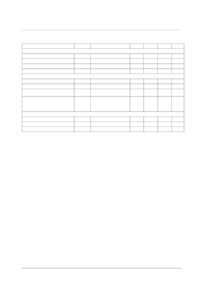
Test Conditions:
R
L
= 10k
, C
L
= 100pF. VDD
= 5V ±10%, V
REF
= 2.048V and VDD
= 3V ±10%, V
REF
= 1.024V over recommended operating free-
air temperature range (unless noted otherwise).
PARAMETER
SYMBOL
TEST CONDITIONS
MIN
TYP
MAX
UNIT
Reference Output (Internal reference)
Low reference voltage
V
REFL
1.003
1.024
1.045
V
High reference voltage
V
REFH
2.027
2.048
2.069
V
Output Current
I
REF
±1
mA
Load capacitance
100
pF
Reference Input (External reference)
Reference input resistance
R
REFIN
10
M
Reference input capacitance
C
REFIN
5
pF
Reference feedthrough
V
REF
= 1V
PP
at 1kHz
+ 1.024V dc, DAC code 0
V
REF
= 0.2V
PP
+ 1.024V dc
DAC code 128
Slow
Fast
-80
dB
Reference input bandwidth
0.525
1.3
MHz
MHz
Digital Inputs
High level input current
I
IH
Input voltage = VDD
1
μ
A
Low level input current
I
IL
Input voltage = 0V
-1
μ
A
Input capacitance
C
I
8
pF
Notes:
1.
Integral non-linearity
(INL) is the maximum deviation of the output from the line between zero and full scale (excluding the
effects of zero code and full scale errors).
Differential non-linearity
(DNL) is the difference between the measured and ideal 1LSB amplitude change of any adjacent two
codes. A guarantee of monotonicity means the output voltage always changes in the same direction (or remains constant) as
the digital input code.
Zero code error
is the voltage output when the DAC input code is zero.
Gain error
is the deviation from the ideal full-scale output excluding the effects of zero code error.
Power supply rejection ratio
is measured by varying VDD from 4.5V to 5.5V and measuring the proportion of this signal
imposed on the zero code error and the gain error.
Zero code error
and
Gain error
temperature coefficients are normalised to full-scale voltage.
Output load regulation
is the difference between the output voltage at full scale with a 10k
load and 2k
load. It is
expressed as a percentage of the full scale output voltage with a 10k
load.
I
DD
is measured while continuously writing code 128 to the DAC. For V
IH
< VDD - 0.7V and V
IL
> 0.7V supply current will
increase.
Slew rate
is for an output change from 10% to 90% of full-scale output voltage, or vice versa. The results are for the lower
value of the rising and falling edge slew rates.
10.
Settling time
is the time taken for the signal to settle to within 0.5LSB of the final measured value for both rising and falling
edges. Limits are ensured by design and characterisation, but are not production tested.
11.
SNR, SNRD, THD
and
SPFDR
are measured on a synthesised sine wave at frequency f
OUT
generated with a sampling
frequency f
s.
2.
3.
4.
5.
6.
7.
8.
9.
相關(guān)PDF資料 |
PDF描述 |
|---|---|
| WM2626CD | Low Power Dual 8-bit Serial Input DAC with Internal Reference |
| WM2626 | Low Power Dual 8-bit Serial Input DAC with Internal Reference |
| WM2627CDT | Quad 8-Bit Serial Input Voltage Output DAC |
| WM2627 | Quad 8-Bit Serial Input Voltage Output DAC |
| WM2627IDT | Quad 8-Bit Serial Input Voltage Output DAC |
相關(guān)代理商/技術(shù)參數(shù) |
參數(shù)描述 |
|---|---|
| WM2627 | 制造商:WOLFSON 制造商全稱:WOLFSON 功能描述:Quad 8-Bit Serial Input Voltage Output DAC |
| WM2627CDT | 制造商:WOLFSON 制造商全稱:WOLFSON 功能描述:Quad 8-Bit Serial Input Voltage Output DAC |
| WM2627IDT | 制造商:WOLFSON 制造商全稱:WOLFSON 功能描述:Quad 8-Bit Serial Input Voltage Output DAC |
| WM2629 | 制造商:WOLFSON 制造商全稱:WOLFSON 功能描述:Octal 8-bit, Serial Input, Voltage Output DAC with Power Down |
| WM2630 | 制造商:WOLFSON 制造商全稱:WOLFSON 功能描述:Octal 12-bit, Serial Input, Voltage Output DAC with Internal Reference |
發(fā)布緊急采購,3分鐘左右您將得到回復(fù)。