- 您現(xiàn)在的位置:買賣IC網(wǎng) > PDF目錄68457 > W3H32M64EA-667SBM (MICROSEMI CORP-PMG MICROELECTRONICS) 32M X 64 DDR DRAM, PBGA208 PDF資料下載
參數(shù)資料
| 型號(hào): | W3H32M64EA-667SBM |
| 廠商: | MICROSEMI CORP-PMG MICROELECTRONICS |
| 元件分類: | DRAM |
| 英文描述: | 32M X 64 DDR DRAM, PBGA208 |
| 封裝: | 16 X 20 MM, 1 MM PITCH, PLASTIC, BGA-208 |
| 文件頁數(shù): | 23/28頁 |
| 文件大小: | 1057K |
| 代理商: | W3H32M64EA-667SBM |
第1頁第2頁第3頁第4頁第5頁第6頁第7頁第8頁第9頁第10頁第11頁第12頁第13頁第14頁第15頁第16頁第17頁第18頁第19頁第20頁第21頁第22頁當(dāng)前第23頁第24頁第25頁第26頁第27頁第28頁
4
White Electronic Designs Corporation (602) 437-1520 www.whiteedc.com
White Electronic Designs
February 2010 2010 White Electronic Designs Corp. All rights reserved
Rev. 0
ADVANCED
White Electronic Designs Corp. reserves the right to change products or specications without notice.
W3H32M64EA-XSBX
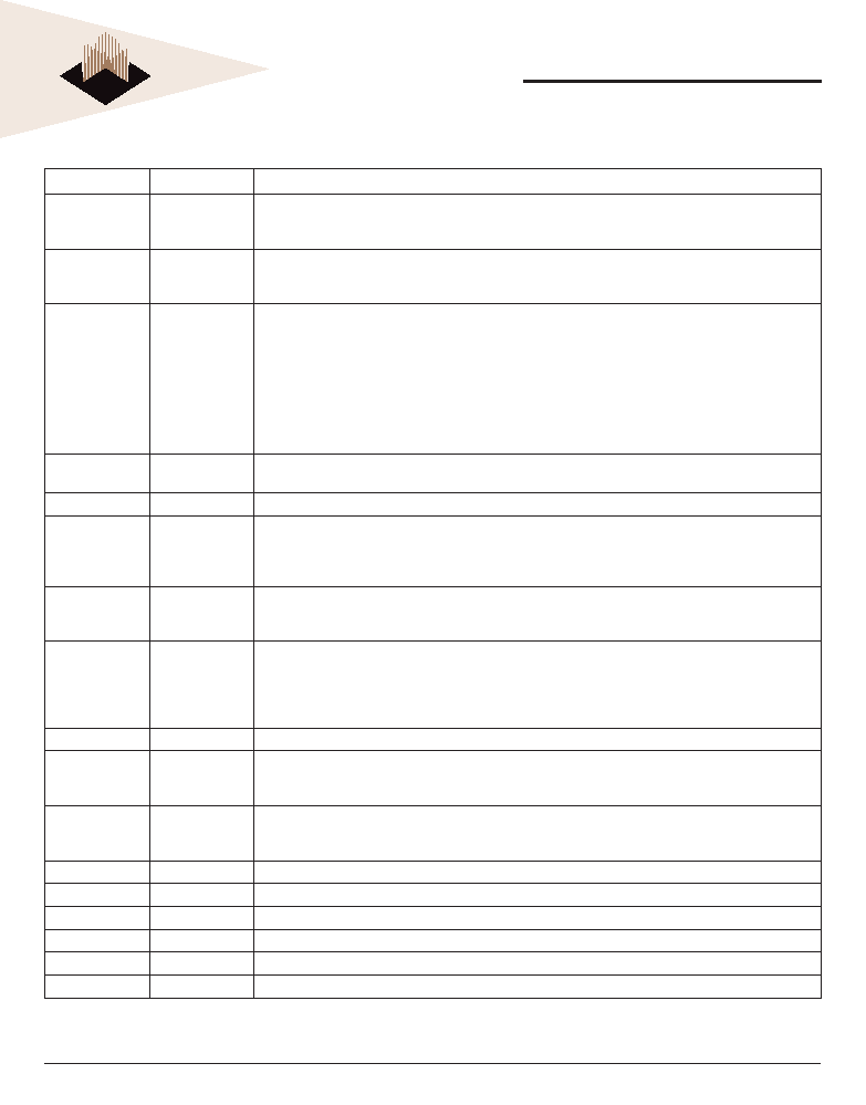
TABLE 1 – BALL DESCRIPTIONS
Symbol
Type
Description
ODT
Input
On-Die termination: ODT (registered HIGH) enables termination resistance internal to the DDR2 SDRAM. When
enabled, ODT is only applied to each of the following balls: DQ0–DQ15, LDM, UDM, LDQS, LDQS#, UDQS, and
UDQS#. The ODT input will be ignored if disabled via the LOAD MODE command.
CK, CK#
Input
Clock: CK and CK# are differential clock inputs. All address and control input signals are sampled on the crossing
of the positive edge of CK and negative edge of CK#. Output data (DQS and DQS/DQS#) is referenced to the
crossings of CK and CK#.
CKE
Input
Clock enable: CKE (registered HIGH) activates and CKE (registered LOW) deactivates clocking circuitry on the
DDR2 SDRAM. The specic circuitry that is enabled/disabled is dependent on the DDR2 SDRAM conguration
and operating mode. CKE LOW provides PRECHARGE power-down mode and SELF-REFRESH action (all banks
idle), or ACTIVE power-down (row active in any bank). CKE is synchronous for power-down entry, Power-down
exit, output disable, and for self refresh entry. CKE is asynchronous for self refresh exit. Input buffers (excluding
CKE, and ODT) are disabled during power-down. Input buffers (excluding CKE) are disabled during self refresh.
CKE is an SSTL_18 input but will detect a LVCMO SLOW level once VCC is applied during rst power-up. After
VREF has become stable during the power on and initialization sequence, it must be maintained for proper
operation of the CKE receiver. For proper SELF-REFRESH operation, VREF must be maintained.
CS#
Input
Chip select: CS# enables (registered LOW) and disables (registered HIGH) the command decoder. All commands
are masked when CS# is registered HIGH.
RAS#, CAS#, WE#
Input
Command inputs: RAS#, CAS#, WE# (along with CS#) dene the command being entered.
LDM, UDM
Input
Input data mask: DM is an input mask signal for write data. Input data is masked when DM is concurrently sampled
HIGH during a WRITE access. DM is sampled on both edges of DQS. Although DM balls are input-only, the DM
loading is designed to match that of DQ and DQS balls. LDM is DM for lower byte DQ0–DQ7 and UDM is DM for
upper byte DQ8–DQ15, of each of IC1-4
BA0–BA1
Input
Bank address inputs: BA0–BA1 dene to which bank an ACTIVE, READ, WRITE, or PRECHARGE command is
being applied. BA0–BA1 dene which mode register including MR, EMR, EMR(2), and EMR(3) is loaded during the
LOAD MODE command.
A0-A12
Input
Address inputs: Provide the row address for ACTIVE commands, and the column address and auto precharge bit
(A10) for READ/WRITE commands, to select one location out of the memory array in the respective bank. A10
sampled during a PRECHARGE command determines whether the PRECHARGE applies to one bank (A10 LOW,
bank selected by BA1–BA0) or all banks (A10 HIGH) The address inputs also provide the op-code during a LOAD
MODE command.
DQ0-63
I/O
Data input/output: Bidirectional data bus
UDQS, UDQS#
I/O
Data strobe for upper byte: Output with read data, input with write data for source synchronous operation. Edge-
aligned with read data, center-aligned with write data. UDQS# is only used when differential data strobe mode is
enabled via the LOAD MODE command.
LDQS, LDQS#
I/O
Data strobe for lower byte: Output with read data, input with write data for source synchronous operation. Edge-
aligned with read data, center-aligned with write data. UDQS# is only used when differential data strobe mode is
enabled via the LOAD MODE command.
VCC
Supply
Power Supply: 1.8V ±0.1V
VCCQ
Supply
Power Supply: I/O; VCCQ is common to VCC
VREF
Supply
SSTL_18 reference voltage.
VSS
Supply
Ground
NC
-
No connect: These balls should be left unconnected.
DNU
-
Future use
相關(guān)PDF資料 |
PDF描述 |
|---|---|
| W3H32M64EA-667SBC | 32M X 64 DDR DRAM, PBGA208 |
| W3H32M72E-667SB2M | 32M X 72 DDR DRAM, 0.65 ns, PBGA208 |
| W3H32M72E-667SBC | 32M X 72 DDR DRAM, 0.65 ns, PBGA208 |
| W3H64M16E-400BC | 64M X 16 DDR DRAM, 0.6 ns, PBGA79 |
| W3H64M64E-400SBC | 64M X 64 DDR DRAM, 0.6 ns, PBGA208 |
相關(guān)代理商/技術(shù)參數(shù) |
參數(shù)描述 |
|---|---|
| W3H32M64E-ES | 制造商:WEDC 制造商全稱:White Electronic Designs Corporation 功能描述:32M x 64 DDR2 SDRAM 208 PBGA Multi-Chip Package |
| W3H32M64E-ESC | 制造商:WEDC 制造商全稱:White Electronic Designs Corporation 功能描述:32M x 64 DDR2 SDRAM 208 PBGA Multi-Chip Package |
| W3H32M64E-ESI | 制造商:WEDC 制造商全稱:White Electronic Designs Corporation 功能描述:32M x 64 DDR2 SDRAM 208 PBGA Multi-Chip Package |
| W3H32M64E-ESM | 制造商:WEDC 制造商全稱:White Electronic Designs Corporation 功能描述:32M x 64 DDR2 SDRAM 208 PBGA Multi-Chip Package |
| W3H32M64E-SB | 制造商:WEDC 制造商全稱:White Electronic Designs Corporation 功能描述:32M x 64 DDR2 SDRAM 208 PBGA Multi-Chip Package |
發(fā)布緊急采購(gòu),3分鐘左右您將得到回復(fù)。