- 您現(xiàn)在的位置:買賣IC網(wǎng) > PDF目錄140365 > W3E16M72SR200BI (WHITE ELECTRONIC DESIGNS CORP) 16M X 72 DDR DRAM, 0.75 ns, PBGA219 PDF資料下載
參數(shù)資料
| 型號: | W3E16M72SR200BI |
| 廠商: | WHITE ELECTRONIC DESIGNS CORP |
| 元件分類: | DRAM |
| 英文描述: | 16M X 72 DDR DRAM, 0.75 ns, PBGA219 |
| 封裝: | 32 X 25 MM, PLASTIC, BGA-219 |
| 文件頁數(shù): | 13/16頁 |
| 文件大?。?/td> | 744K |
| 代理商: | W3E16M72SR200BI |
6
White Electronic Designs Corporation (602) 437-1520 www.wedc.com
White Electronic Designs
W3E16M72SR-XBX
February 2005
Rev. 2
EXTENDED MODE REGISTER
The extended mode register controls functions beyond
those controlled by the mode register; these additional
functions are DLL enable/disable, output drive strength,
and QFC#. These functions are controlled via the bits
shown in Figure 5. The extended mode register is
programmed via the LOAD MODE REGISTER command
to the mode register (with BA0 = 1 and BA1 = 0) and
will retain the stored information until it is programmed
again or the device loses power. The enabling of the DLL
should always be followed by a LOAD MODE REGISTER
command to the mode register (BA0/BA1 both LOW) to
reset the DLL.
The extended mode register must be loaded when all
banks are idle and no bursts are in progress, and the
controller must wait the specied time before initiating
any subsequent operation. Violating either of these
requirements could result in unspecied operation.
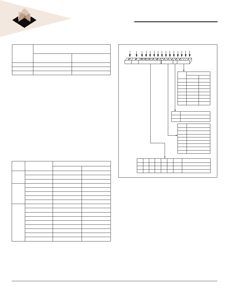
FIGURE 3 – MODE REGISTER DEFINITION
M3 = 0
2
4
8
Reserved
M3 = 1
2
4
8
Reserved
Operating Mode
Normal Operation
Normal Operation/Reset DLL
All other states reserved
00
Valid
0
1
Burst Type
Sequential
Interleaved
CAS Latency
Reserved
2
Reserved
2.5
Reserved
Burst Length
M0
0
1
0
1
0
1
0
1
Burst Length
CAS Latency BT
A9
A7 A6
A5 A4 A3
A8
A2
A1 A0
Mode Register (Mx)
Address Bus
M1
0
1
0
1
M2
0
1
M3
M4
0
1
0
1
0
1
0
1
M5
0
1
0
1
M6
0
1
M6-M0
M8
M7
Operating Mode
A10
A11
* M14 and M13
(BA0 and BA1 must be
"0, 0" to select
the base mode register
(vs. the extended
mode register).
0*
BA0
BA1
Reserved
M9
M10
M11
0
10
0
--
-
A12
M12
0
-
TABLE 2 – CAS LATENCY
SPEED
ALLOWABLE OPERATING
FREQUENCY (MHz)
CAS
LATENCY = 2
CAS
LATENCY = 2.5
-200
≤ 75
≤ 100
-225
≤ 100
≤ 112.5
-250
≤ 100
≤ 125
OPERATING MODE
The normal operating mode is selected by issuing a MODE
REGISTER SET command with bits A7-A12 each set to
zero, and bits A0-A6 set to the desired values. A DLL reset
is initiated by issuing a MODE REGISTER SET command
with bits A7 and A9-A12 each set to zero, bit A8 set to one,
and bits A0-A6 set to the desired values. Although not
required, JEDEC specications recommend when a LOAD
MODE REGISTER command is issued to reset the DLL, it
should always be followed by a LOAD MODE REGISTER
command to select normal operating mode.
All other combinations of values for A7-A12 are reserved
for future use and/or test modes. Test modes and reserved
states should not be used because unknown operation or
incompatibility with future versions may result.
TABLE 1 – BURST DEFINITION
Burst
Length
Starting Column
Address
Order of Accesses Within a Burst
Type = Sequential
Type = Interleaved
2
A0
0
0-1
1
1-0
4
A1
A0
0
0-1-2-3
0
1
1-2-3-0
1-0-3-2
1
0
2-3-0-1
1
3-0-1-2
3-2-1-0
8
A2
A1
A0
0
0-1-2-3-4-5-6-7
0
1
1-2-3-4-5-6-7-0
1-0-3-2-5-4-7-6
0
1
0
2-3-4-5-6-7-0-1
2-3-0-1-6-7-4-5
0
1
3-4-5-6-7-0-1-2
3-2-1-0-7-6-5-4
1
0
4-5-6-7-0-1-2-3
1
0
1
5-6-7-0-1-2-3-4
5-4-7-6-1-0-3-2
1
0
6-7-0-1-2-3-4-5
6-7-4-5-2-3-0-1
1
7-0-1-2-3-4-5-6
7-6-5-4-3-2-1-0
NOTES:
1.
For a burst length of two, A1-Ai select two-data-element block; A0 selects the
starting column within the block.
2.
For a burst length of four, A2-Ai select four-data-element block; A0-1 select the
starting column within the block.
3.
For a burst length of eight, A3-Ai select eight-data-element block; A0-2 select the
starting column within the block.
4.
Whenever a boundary of the block is reached within a given sequence above, the
following access wraps within the block.
相關PDF資料 |
PDF描述 |
|---|---|
| W764M32V100SBI | 64M X 32 FLASH 3V PROM, 100 ns, PBGA107 |
| W25Q16CLSSIG | 16M X 1 SPI BUS SERIAL EEPROM, PDSO8 |
| W25Q40BWUXIG | 4M X 1 SPI BUS SERIAL EEPROM, PDSO8 |
| WF128K32NA-200HM | 512K X 8 FLASH 12V PROM MODULE, 200 ns, CHIP66 |
| WS512K32N-45HI | 2M X 8 MULTI DEVICE SRAM MODULE, 45 ns, CHIP66 |
相關代理商/技術參數(shù) |
參數(shù)描述 |
|---|---|
| W3E16M72SR-200BI | 制造商:WEDC 制造商全稱:White Electronic Designs Corporation 功能描述:16Mx72 Registered DDR SDRAM |
| W3E16M72SR-200BM | 制造商:WEDC 制造商全稱:White Electronic Designs Corporation 功能描述:16Mx72 Registered DDR SDRAM |
| W3E16M72SR-225BC | 制造商:WEDC 制造商全稱:White Electronic Designs Corporation 功能描述:16Mx72 Registered DDR SDRAM |
| W3E16M72SR-225BI | 制造商:WEDC 制造商全稱:White Electronic Designs Corporation 功能描述:16Mx72 Registered DDR SDRAM |
| W3E16M72SR-225BM | 制造商:WEDC 制造商全稱:White Electronic Designs Corporation 功能描述:16Mx72 Registered DDR SDRAM |
發(fā)布緊急采購,3分鐘左右您將得到回復。