- 您現(xiàn)在的位置:買賣IC網(wǎng) > PDF目錄202172 > V59C1512164QCF3I (PROMOS TECHNOLOGIES INC) 32M X 16 DDR DRAM, 0.45 ns, PBGA84 PDF資料下載
參數(shù)資料
| 型號(hào): | V59C1512164QCF3I |
| 廠商: | PROMOS TECHNOLOGIES INC |
| 元件分類: | DRAM |
| 英文描述: | 32M X 16 DDR DRAM, 0.45 ns, PBGA84 |
| 封裝: | ROHS COMPLIANT, MO-207, FBGA-84 |
| 文件頁(yè)數(shù): | 64/76頁(yè) |
| 文件大?。?/td> | 1192K |
| 代理商: | V59C1512164QCF3I |
第1頁(yè)第2頁(yè)第3頁(yè)第4頁(yè)第5頁(yè)第6頁(yè)第7頁(yè)第8頁(yè)第9頁(yè)第10頁(yè)第11頁(yè)第12頁(yè)第13頁(yè)第14頁(yè)第15頁(yè)第16頁(yè)第17頁(yè)第18頁(yè)第19頁(yè)第20頁(yè)第21頁(yè)第22頁(yè)第23頁(yè)第24頁(yè)第25頁(yè)第26頁(yè)第27頁(yè)第28頁(yè)第29頁(yè)第30頁(yè)第31頁(yè)第32頁(yè)第33頁(yè)第34頁(yè)第35頁(yè)第36頁(yè)第37頁(yè)第38頁(yè)第39頁(yè)第40頁(yè)第41頁(yè)第42頁(yè)第43頁(yè)第44頁(yè)第45頁(yè)第46頁(yè)第47頁(yè)第48頁(yè)第49頁(yè)第50頁(yè)第51頁(yè)第52頁(yè)第53頁(yè)第54頁(yè)第55頁(yè)第56頁(yè)第57頁(yè)第58頁(yè)第59頁(yè)第60頁(yè)第61頁(yè)第62頁(yè)第63頁(yè)當(dāng)前第64頁(yè)第65頁(yè)第66頁(yè)第67頁(yè)第68頁(yè)第69頁(yè)第70頁(yè)第71頁(yè)第72頁(yè)第73頁(yè)第74頁(yè)第75頁(yè)第76頁(yè)
67
ProMOS TECHNOLOGIES
V59C1512(404/804/164)QC*I
V59C1512(404/804/164)QC*I Rev. 1.1 April 2008
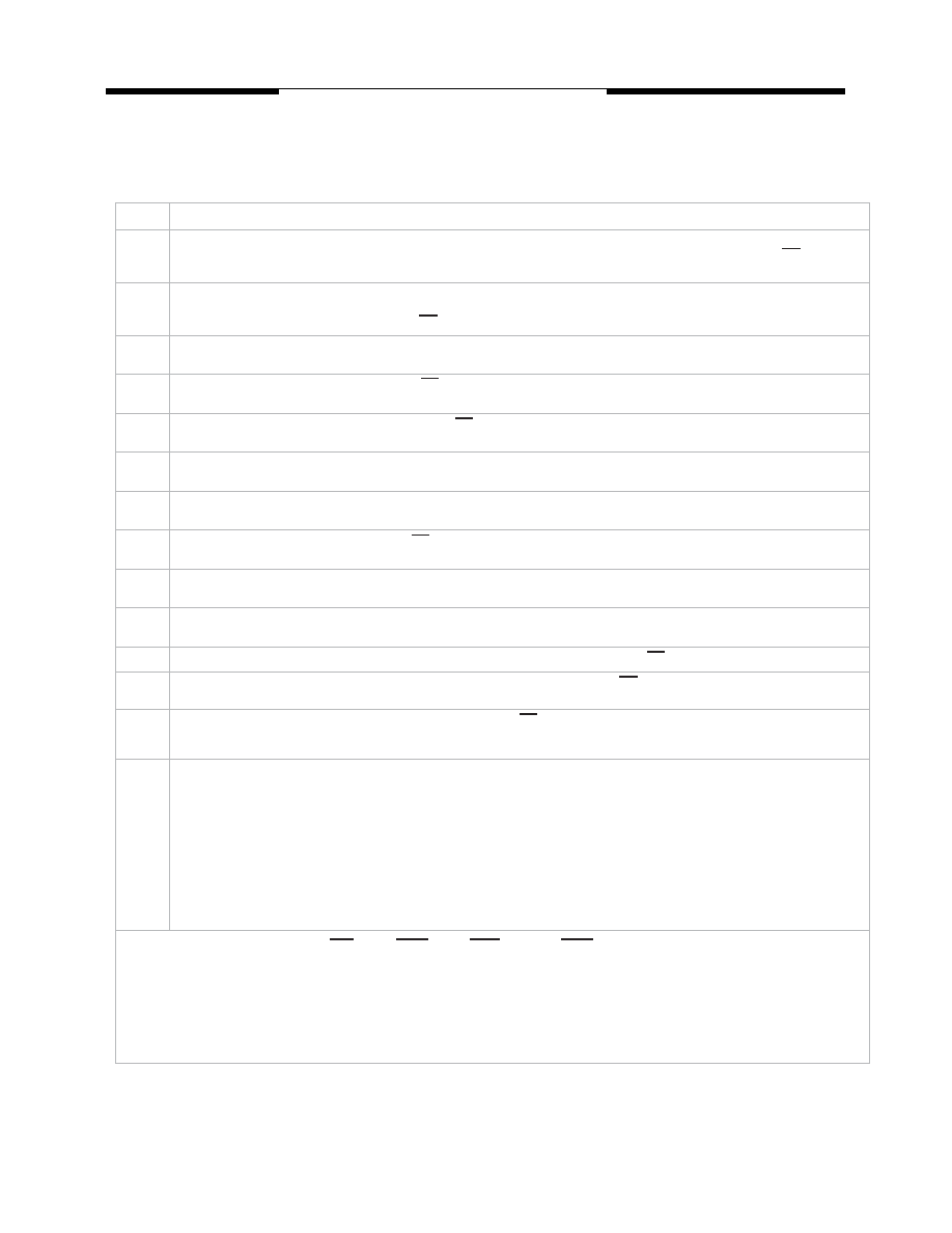
IDD Measurement Cond itio ns
(-40 °C < T
+85 °C ; VDDQ = 1.8V ± 0.1V; VDD = 1.8V ± 0.1V)
Symbol
Parameter/Condition
IDD0
Operating C ur rent - One bank Active - Precharge
tRC = tRCmin; tCK =tCKmin. ; Databus inputs are SWITCHING; Address and control inputs are SWITCHING, CS = HIGH
between valid commands.
IDD1
Operating C ur rent - One bank Ac ti ve - Read - Precharg e
One bank is accessed with tRCmin , BL = 4, tCK = tCKmin, AL = 0, CL = CLmin.;
Address and control inputs are SWITCHING,CS = HIGH between valid commands; lout = 0 mA.
IDD2P
Precharg e Power-Do wn Curre nt: all banks idle; power-down mode; CKE is LOW; tCK = tCKmin.; Data Bus inputs are
FLOATING.
IDD2N
Precharge Standby Current: all banks idle; CS is HIGH; CKE is HIGH; tCK = tCKmin.; Address and control inputs
are SWITCHING; Data Bus inputs are SWITCHING.
.
IDD2Q
Precharge Quiet Standby Current: all banks idle; CS is HIGH; CKE is HIGH; tCK = tCKmin.; Address and control inputs are
STABLE; Data Bus inputs are FLOATING.
IDD3P
Ac ti ve Power-Do wn Curre nt: all banks open; CKE is LOW; Address and control inputs are STABLE; Data Bus inputs are
FLOATING. MRS A12 bit is set to “0”( Fast Power-down Exit);
IDD3P
Ac ti ve Power-Do wn Curre nt: all banks open; CKE is LOW; Address and control inputs are STABLE; Data Bus inputs are
FLOATING. MRS A12 bit is set to “1”( Slow Power-down Exit);
IDD3N
Act ive Standby Current: all banks open; CS is HIGH; CKE is HIGH; tRC = tRASmax; tCK = tCKmin.;
Address and control inputs are SWITCHING; Data Bus inputs are SWITCHING.
IDD4R
Operating Curre nt - Burs t Read: all banks active; continuous burst reads; BL = 4;AL = 0, CL = CLmin.; tCK = tCKmin.;
Address and control inputs are SWITCHING; Data Bus inputs are SWITCHING; IOUT = 0mA.
IDD4W
Operating Curre nt - Burs t Write: all banks active; continuous burst writes; BL = 4;AL = 0, CL = CLmin.; tCK = tCKmin.;
Address and control inputs are SWITCHING; Data Bus inputs are SWITCHING; IOUT = 0mA.
IDD5B Burs t Au to-Refresh Current: Refresh command at tRFC = tRFCmin, tCK = tCKmin, CS is HIGH between valid commands
IDD5D
Distri buted Au to-Refre sh Curre nt: Refresh command at tREFI; tCK = tCKmin, CS is HIGH between valid commands;
CKE is LOW except during tRFCmin.
IDD6
Self-Refre sh Curre nt: CKE
0.2V; external clock off, CK and CK at 0V; tCK = tCKmin; Address and control inputs are
FLOATING;
Data Bus inputs are FLOATING.
IDD7
Operating Bank Interleave Read Current:
1. All bank interleaving with BL = 4; BL = 4, CL = CLmin.;tRCD = tRCDmin.; tRRD = tRRDmin.;AL = tRCD - 1, Iout = 0 mA.
Address and control inputs are stable during DESELECT; Data Bus inputs are SWITCHING.
2. Timing pattern:
- DDR2 -400 (200Mhz, CL=3) : tck = 5 ns, BL = 4, tRCD = 3 * tck, AL = 2 * tck, tRC = 12 * tck
Read : A0 RA0 A1 RA1 A2 RA2 A3 RA3 D D D D
- DDR2 -533 (266Mhz, CL=4) : tck = 3.7 ns, BL = 4, tRCD = 4 * tck, AL = 3 * tck, tRC = 16 * tck
Read : A0 RA0 D A1 RA1 D A2 RA2 D A3 RA3 D D D D D
- DDR2 -667 (333Mhz, CL=4) : tck = 3 ns, BL = 4, tRCD = 4 * tck, AL = 3 * tck, tRC = 19 * tck
Read : A0 RA0 D D A1 RA1 D D A2 RA2 D D A3 RA3 D D D D D
1. Data Bus consists of DQ, DM, DQS, DQS, RDQS, RDQS, LDQS, LDQS, UDQS and UDQS.
2. Definitions for IDD :
LOW is defined as VIN <= VILAC(max.); HIGH is defined as VIN >= VIHAC(min.);
STABLE is defined as inputs are stable at a HIGH or LOW level
FLOATING is defined as inputs are VREF
SWITCHING is defined as inputs are changing between HIGH and LOW every other clock for adress and control signals, and
inputs changing 50% of each data trasnfer for DQ signals.
3. Legend : A=Activate, RA=Read with Auto-Precharge, D=DESELECT
_
<
A
相關(guān)PDF資料 |
PDF描述 |
|---|---|
| V59C1G01168QBLJ-25I | DDR DRAM, PBGA84 |
| V59C1G01408QAUP25A | 256M X 4 DDR DRAM, PBGA68 |
| V59C1512164QALJ25AH | 32M X 16 DDR DRAM, PBGA92 |
| V59C1512164QALP37I | 32M X 16 DDR DRAM, PBGA92 |
| V59C1512164QAUJ5I | 32M X 16 DDR DRAM, PBGA92 |
相關(guān)代理商/技術(shù)參數(shù) |
參數(shù)描述 |
|---|---|
| V59C1512164QDJ25 | 制造商:ProMOS 功能描述:32M*16 DDRII, 1.8V, BGA, 400MHz, Green Part 制造商:ProMOS Technologies INC. 功能描述:32M*16 DDRII, 1.8V, BGA, 400MHz, Green Part |
| V59C1512164QDJ25A | 制造商:ProMOS 功能描述:32M*16 DDRII, 1.8V, BGA, 800MHz, Green Part, CL6 制造商:ProMOS Technologies INC. 功能描述:32M*16 DDRII, 1.8V, BGA, 800MHz, Green Part, CL6 |
| V59C1512164QDJ25I | 制造商:ProMOS 功能描述:32M*16 DDRII, 1.8V, BGA, 333MHz, Green Part, 制造商:ProMOS Technologies INC. 功能描述:32M*16 DDRII, 1.8V, BGA, 333MHz, Green Part, |
| V59C1512164QDJ3 | 制造商:ProMOS 功能描述:32M*16 DDRII, 1.8V, BGA, 333MHz, Green Part 制造商:ProMOS Technologies INC. 功能描述:32M*16 DDRII, 1.8V, BGA, 333MHz, Green Part |
| V59C1512164QDJ3I | 制造商:ProMOS 功能描述:32M*16 DDRII, 1.8V, BGA, 333MHz, Green Part, 制造商:ProMOS Technologies INC. 功能描述:32M*16 DDRII, 1.8V, BGA, 333MHz, Green Part, |
發(fā)布緊急采購(gòu),3分鐘左右您將得到回復(fù)。