- 您現(xiàn)在的位置:買賣IC網(wǎng) > PDF目錄361602 > UT8Q1024K8-UWX (Aeroflex Inc.) high-performance 1M byte (8Mbit) CMOS static RAM PDF資料下載
參數(shù)資料
| 型號(hào): | UT8Q1024K8-UWX |
| 廠商: | Aeroflex Inc. |
| 英文描述: | high-performance 1M byte (8Mbit) CMOS static RAM |
| 中文描述: | 高性能1M字節(jié)(8Mbit)的CMOS靜態(tài)RAM |
| 文件頁數(shù): | 2/15頁 |
| 文件大?。?/td> | 238K |
| 代理商: | UT8Q1024K8-UWX |
2
PIN NAMES
Notes:
1. To avoid bus contention, on the DQ(7:0) bus, only one En can be driven low
simultaneously while G is low.
DEVICE OPERATION
Each die in the UT8Q1024K8 has three control inputs called
Enable (En), Write Enable (Wn), and Output Enable (G); 19
address inputs, A(18:0); and eight bidirectional data lines,
DQ(7:0). The device enable (En) controls device selection,
active, and standby modes. Asserting En enables the device,
causes I
DD
to rise to its active value, and decodes the 19 address
inputs to each memory die. Wn controls read and write
operations. During a read cycle, G must be asserted to enable
the outputs.
Table 1. Device Operation Truth Table
Notes:
1. “X” is defined as a “don’t care” condition.
2. Device active; outputs disabled.
READ CYCLE
A combination of Wn greater than V
IH
(min) with En and G less
than V
IL
(max) defines a read cycle. Read access time is
measured from the latter of device enable, output enable, or valid
address to valid data output.
SRAM Read Cycle 1, the Address Access is initiated by a change
in address inputs while the chip is enabled with G asserted and
Wn deasserted. Valid data appears on data outputs DQ(7:0) after
the specified t
AVQV
is satisfied. Outputs remain active
throughout the entire cycle. As long as device enable and output
enable are active, the address inputs may change at a rate equal
to the minimum read cycle time (t
AVAV
).
SRAM Read Cycle 2, the Chip Enable-controlled Access is
initiated by En going active while G remains asserted, Wn
remains deasserted, and the addresses remain stable for the
entire cycle. After the specified t
ETQV
is satisfied, the eight-bit
word addressed by A(18:0) is accessed and appears at the data
outputs DQ(7:0).
SRAM Read Cycle 3, the Output Enable-controlled Access is
initiated by G going active while En is asserted, Wn is
deasserted, and the addresses are stable. Read access time is
t
GLQV
unless t
AVQV
or t
ETQV
have not been satisfied.
A(18:0)
Address
DQ(7:0)
Data Input/Output
En
Device Enable
Wn
WriteEnable
G
Output Enable
V
DD
Power
V
SS
Ground
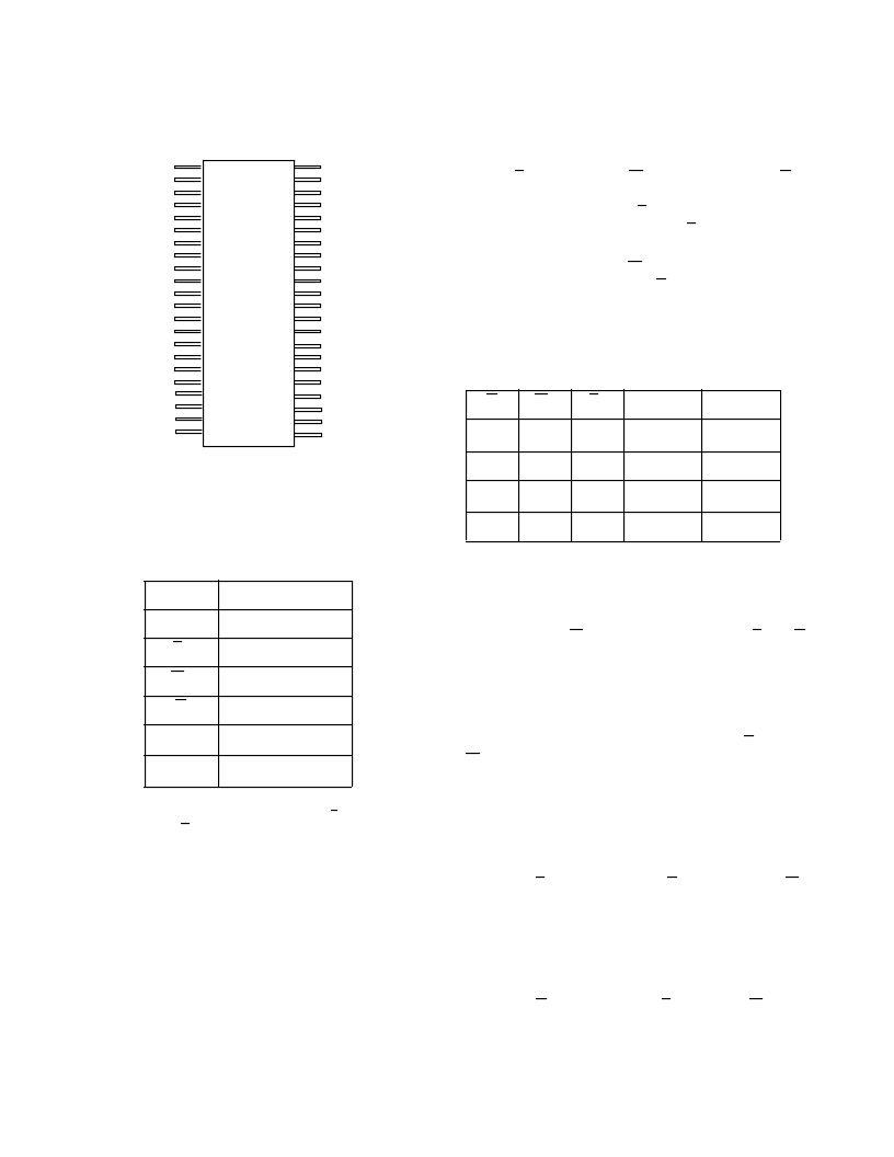
Figure 2. 25ns SRAM Pinout (44)
1
2
3
4
5
6
7
8
9
10
11
12
14
15
16
17
18
19
20
21
22
44
43
42
41
40
39
38
37
36
35
34
33
32
31
30
29
28
27
26
25
24
23
NC
E2
NC
A18
A17
A16
A15
G
DQ7
DQ6
V
SS
V
DD
DQ5
DQ4
A14
A13
A12
A11
A10
NC
NC
NC
NC
NC
A0
A1
A2
A3
A4
E1
DQ0
DQ1
V
DD
V
SS
DQ2
DQ3
W1
A5
A6
A7
A8
A9
W2
NC
G
Wn
En
I/O Mode
Mode
X
1
X
1
3-state
Standby
X
0
0
Data in
Write
1
1
0
3-state
Read
2
0
1
0
Data out
Read
相關(guān)PDF資料 |
PDF描述 |
|---|---|
| UT8Q512K32-SWC | 16Megabit SRAM MCM |
| UT8Q512K32 | 16Megabit SRAM MCM |
| UT8Q512K32-SPC | 16Megabit SRAM MCM |
| UT912E | ENCODER FOR REMOTE CONTROLLER |
| UT912E-D14-T | ENCODER FOR REMOTE CONTROLLER |
相關(guān)代理商/技術(shù)參數(shù) |
參數(shù)描述 |
|---|---|
| UT8Q512-25UCA | 制造商:未知廠家 制造商全稱:未知廠家 功能描述:SRAM|512KX8|CMOS| RAD HARD|FP|36PIN|CERAMIC |
| UT8Q512-25UCC | 制造商:未知廠家 制造商全稱:未知廠家 功能描述:SRAM|512KX8|CMOS| RAD HARD|FP|36PIN|CERAMIC |
| UT8Q512K32 | 制造商:AEROFLEX 制造商全稱:AEROFLEX 功能描述:16Megabit SRAM MCM |
| UT8Q512K32-SPC | 制造商:AEROFLEX 制造商全稱:AEROFLEX 功能描述:16Megabit SRAM MCM |
| UT8Q512K32-SWC | 制造商:AEROFLEX 制造商全稱:AEROFLEX 功能描述:16Megabit SRAM MCM |
發(fā)布緊急采購,3分鐘左右您將得到回復(fù)。