- 您現在的位置:買賣IC網 > PDF目錄379503 > UPD753016GK-XXX-BE9 (NEC Corp.) MICROCONTROLLER|4-BIT|UPD75XL CPU|CMOS|TQFP|80PIN|PLASTIC PDF資料下載
參數資料
| 型號: | UPD753016GK-XXX-BE9 |
| 廠商: | NEC Corp. |
| 英文描述: | MICROCONTROLLER|4-BIT|UPD75XL CPU|CMOS|TQFP|80PIN|PLASTIC |
| 中文描述: | 單片機| 4位| UPD75XL的CPU |的CMOS | TQFP封裝| 80腳|塑料 |
| 文件頁數: | 40/80頁 |
| 文件大?。?/td> | 569K |
| 代理商: | UPD753016GK-XXX-BE9 |
第1頁第2頁第3頁第4頁第5頁第6頁第7頁第8頁第9頁第10頁第11頁第12頁第13頁第14頁第15頁第16頁第17頁第18頁第19頁第20頁第21頁第22頁第23頁第24頁第25頁第26頁第27頁第28頁第29頁第30頁第31頁第32頁第33頁第34頁第35頁第36頁第37頁第38頁第39頁當前第40頁第41頁第42頁第43頁第44頁第45頁第46頁第47頁第48頁第49頁第50頁第51頁第52頁第53頁第54頁第55頁第56頁第57頁第58頁第59頁第60頁第61頁第62頁第63頁第64頁第65頁第66頁第67頁第68頁第69頁第70頁第71頁第72頁第73頁第74頁第75頁第76頁第77頁第78頁第79頁第80頁
40
μ
PD753012, 753016, 753017
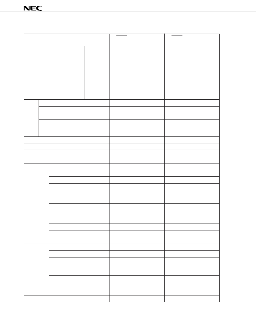
Table 9-1. Status of Each Device After Reset (1/2)
Hardware
RESET Signal Generation
in Standby Mode
RESET Signal Generation
in Operation
Program counter (PC)
μ
PD753012,
753016
Sets the low-order 6 bits of
program memory’s address
0000H to the PC13-PC8 and the
contents of address 0001H to
the PC7-PC0.
Sets the low-order 6 bits of
program memory’s address
0000H to the PC13-PC8 and the
contents of address 0001H to
the PC7-PC0.
μ
PD753017
Sets the low-order 7 bits of
program memory’s address
0000H to the PC14-PC8 and the
contents of address 0001H to
the PC7-PC0.
Sets the low-order 7 bits of
program memory’s address
0000H to the PC14-PC8 and the
contents of address 0001H to
the PC7-PC0.
PSW
Carry flag (CY)
Held
Undefined
Skip flag (SK0-SK2)
0
0
Interrupt status flag (IST0)
0
0
Bank enable flag (MBE, RBE)
Sets the bit 6 of program
memory’s address 0000H to
the RBE and bit 7 to the MBE.
Sets the bit 6 of program
memory’s address 0000H to
the RBE and bit 7 to the MBE.
Stack pointer (SP)
Undefined
Undefined
Stack bank select register (SBS)
1000B
1000B
Data memory (RAM)
Held
Undefined
General-purpose register (X, A, H, L, D, E, B, C)
Held
Undefined
Bank select register (MBS, RBS)
0, 0
0, 0
Basic interval/
Counter (BT)
Undefined
Undefined
watchdog
Mode register (BTM)
0
0
timer
Watchdog timer enable flag (WDTM)
0
0
Timer/event
Counter (T0)
0
0
counter (T0)
Modulo register (TMOD0)
FFH
FFH
Mode register (TM0)
0
0
TOE0, TOUT F/F
0, 0
0, 0
Timer/event
Counter (T1)
0
0
counter (T1)
Modulo register (TMOD1)
FFH
FFH
Mode register (TM1)
0
0
TOE1, TOUT F/F
0, 0
0, 0
Timer/event
Counter (T2)
0
0
counter (T2)
Modulo register (TMOD2)
FFH
FFH
High level period setting modulo
register (TMOD2H)
FFH
FFH
Mode register (TM2)
0
0
TOE2, TOUT F/F
0, 0
0, 0
REMC, NRZ, NRZB
0, 0, 0
0, 0, 0
TGCE
0
0
Watch timer
Mode register (WM)
0
0
相關PDF資料 |
PDF描述 |
|---|---|
| UPD75304B | 4-BIT SINGLE-CHIP MICROCOMPUTER |
| UPD75304BGC | 4-BIT SINGLE-CHIP MICROCOMPUTER |
| UPD75304BGF | 4-BIT SINGLE-CHIP MICROCOMPUTER |
| UPD75304BGK | 4-BIT SINGLE-CHIP MICROCOMPUTER |
| UPD75306B | 4-BIT SINGLE-CHIP MICROCOMPUTER |
相關代理商/技術參數 |
參數描述 |
|---|---|
| UPD75304GF-407-3B9 | 制造商:Renesas Electronics Corporation 功能描述: |
| UPD75306G182 | 制造商:Panasonic Industrial Company 功能描述:IC |
| UPD75308F478 | 制造商:Panasonic Industrial Company 功能描述:IC |
| UPD75308G699 | 制造商:Panasonic Industrial Company 功能描述:IC |
| UPD753204013 | 制造商:Panasonic Industrial Company 功能描述:IC |
發(fā)布緊急采購,3分鐘左右您將得到回復。