- 您現(xiàn)在的位置:買賣IC網(wǎng) > PDF目錄378742 > UPD64 (NEC Corp.) 4-BIT SINGLE-CHIP MICROCONTROLLER FOR INFRARED REMOTE CONTROL TRANSMISSION PDF資料下載
參數(shù)資料
| 型號(hào): | UPD64 |
| 廠商: | NEC Corp. |
| 英文描述: | 4-BIT SINGLE-CHIP MICROCONTROLLER FOR INFRARED REMOTE CONTROL TRANSMISSION |
| 中文描述: | 4位單片機(jī)的紅外遙控傳輸 |
| 文件頁數(shù): | 60/68頁 |
| 文件大小: | 301K |
| 代理商: | UPD64 |
第1頁第2頁第3頁第4頁第5頁第6頁第7頁第8頁第9頁第10頁第11頁第12頁第13頁第14頁第15頁第16頁第17頁第18頁第19頁第20頁第21頁第22頁第23頁第24頁第25頁第26頁第27頁第28頁第29頁第30頁第31頁第32頁第33頁第34頁第35頁第36頁第37頁第38頁第39頁第40頁第41頁第42頁第43頁第44頁第45頁第46頁第47頁第48頁第49頁第50頁第51頁第52頁第53頁第54頁第55頁第56頁第57頁第58頁第59頁當(dāng)前第60頁第61頁第62頁第63頁第64頁第65頁第66頁第67頁第68頁
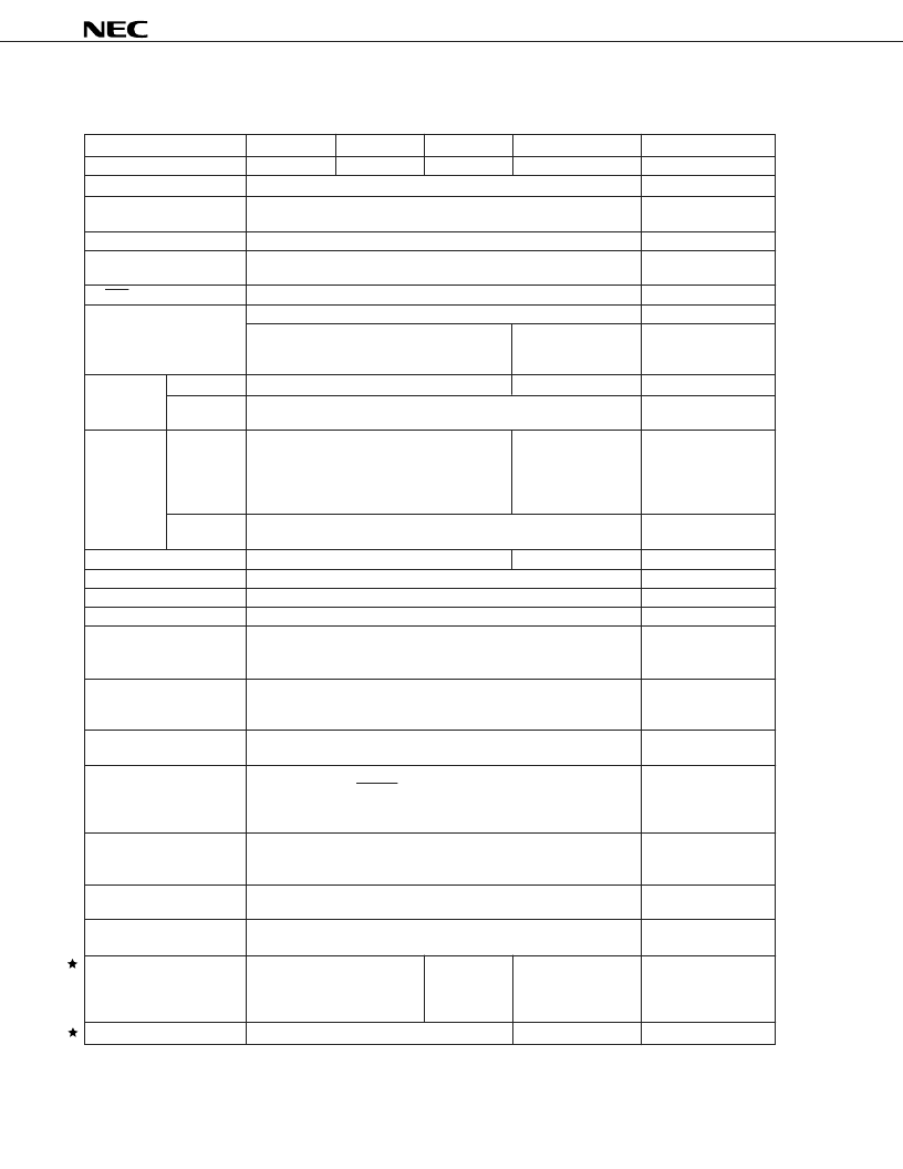
60
μ
PD63, 63A, 64
Item
μ
PD63
512
×
10 bits
32
×
4 bits
1 level (multiplexed with RF of RAM)
μ
PD63A
768
×
10 bits
μ
PD64
μ
PD6134
1002
×
10 bits
μ
PD6600A
512
×
10 bits
32
×
5 bits
3 levels
(multiplexed with RAM)
8
×
4 = 32 keys
Read by left shift
instruction
Output
Ceramic oscillation
ROM capacity
RAM capacity
Stack
1002
×
10 bits
Key matrix
S
0
(S-IN) input
8
×
6 = 48 keys
Read by P
01
register (with function to release standby mode)
S
1
/LED (S-OUT)
Clock frequency
I/O (with function to release standby mode)
Ceramic oscillation
f
X
= 2.4 to 8 MHz
f
X
= 2.4 to 4 MHz (with POC circuit)
f
X
= 300 kHz to 1 MHz f
X
= 400 to 500 kHz
f
X
= 300 to 500 kHz
(with POC circuit)
f
X
/8, f
X
/16
Timer
Clock
Count start
f
X
/64, f
X
/128
Writing count value
f
X
/8
Writing count value
and P1 register value
f
X
/8, f
X
/12
Carrier
Frequency
f
X
/8, f
X
/64, f
X
/96 (timer clock: f
X
/64)
f
X
/16, f
X
/128, f
X
/192 (timer clock: f
X
/128)
No carrier
f
X
, f
X
/8, f
X
/12
(timer clock: f
X
/8)
f
X
/2, f
X
/16, f
X
/24
(timer clock: f
X
/16)
No carrier
Output start
Synchronized with timer
Not synchronized
with timer
16
μ
s (f
X
= 500 kHz)
Provided
Provided
n = 0 to F
HALT/STOP mode
set by P1 register
value
HALT instruction
executed regardless
of status of F
Provided
Instruction execution time
Relative branch instruction
Left shift instruction
“MOV Rn, @RO” instruction
Standby mode
(HALT instruction)
8
μ
s (f
X
= 8 MHz)
None
None
n = 1 to F
HALT mode for timer only.
STOP mode for only releasing K
I
(K
I/O
high-level output or K
I/O0
high-level output)
HALT instruction not executed when F = 1
8
μ
s (f
X
= 1 MHz)
Relation between HALT
instruction execution and
status flag (F)
Reset function by charging/
discharging capacitor
POC circuit
None
Mask option
Low level output to RESET pin on detection
Provided (low-voltage
detection circuit)
Low level output to
S-OUT pin on detection
Pull-down resistor
Variable duty
Hang-up detection
V
DD
= 2.2 to 3.6 V
Mask option
POC circuit only
(Circuits other than POC circuit are set by software.)
Supply voltage
V
DD
= 1.8 to 3.6 V
V
DD
= 2.2 to 3.6 V (with POC circuit)
T
A
= –40 to +85
°
C
T
A
= –20 to +70
°
C (with POC circuit)
20-pin plastic SOP
Operating temperature
T
A
= –20 to +70
°
C
Package
20-pin plastic 20-pin plastic SOP
SOP
20-pin plastic
SSOP
μ
PD61P34B
20-pin plastic SOC
20-pin plastic shrink
DIP
One-time PROM model
μ
PD6P4B
μ
PD61P24
APPENDIX B. FUNCTIONAL COMPARISON BETWEEN
μ
PD63 SUBSERIES AND OTHER
SUBSERIES
相關(guān)PDF資料 |
PDF描述 |
|---|---|
| UPD6451A | UPD6451A Data Sheet | Data Sheet[12/1995] |
| UPD6451ACX-001 | On-Screen Display Circuit |
| UPD6451AGT-101 | On-Screen Display Circuit |
| UPD6451AGT-301 | On-Screen Display Circuit |
| UPD6452CS-002 | On-Screen Display Circuit |
相關(guān)代理商/技術(shù)參數(shù) |
參數(shù)描述 |
|---|---|
| UPD64015AGM-UEU-A | 制造商:Renesas Electronics Corporation 功能描述: |
| UPD64031AGJ-8EN(A) | 制造商:Renesas Electronics Corporation 功能描述: |
| UPD64082GF-3BA | 制造商:Renesas Electronics Corporation 功能描述: |
| UPD64084 | 制造商:NEC 制造商全稱:NEC 功能描述:THREE-DIMENSIONAL Y/C SEPARATION LSI WITH ON-CHIP MEMORY |
| uPD64084GC-8EA-A | 制造商:Renesas Electronics 功能描述:Tray |
發(fā)布緊急采購,3分鐘左右您將得到回復(fù)。