- 您現(xiàn)在的位置:買賣IC網(wǎng) > PDF目錄300051 > UNR-3.3/10-D12SM 1-OUTPUT 33 W DC-DC REG PWR SUPPLY MODULE PDF資料下載
參數(shù)資料
| 型號: | UNR-3.3/10-D12SM |
| 元件分類: | 電源模塊 |
| 英文描述: | 1-OUTPUT 33 W DC-DC REG PWR SUPPLY MODULE |
| 文件頁數(shù): | 3/10頁 |
| 文件大小: | 239K |
| 代理商: | UNR-3.3/10-D12SM |
UNR Series
N O N - I S O L A T E D , 1 8 - 3 3 W , 5 & 1 2 V - I N P U T D C / D C C O N V E R T E R S
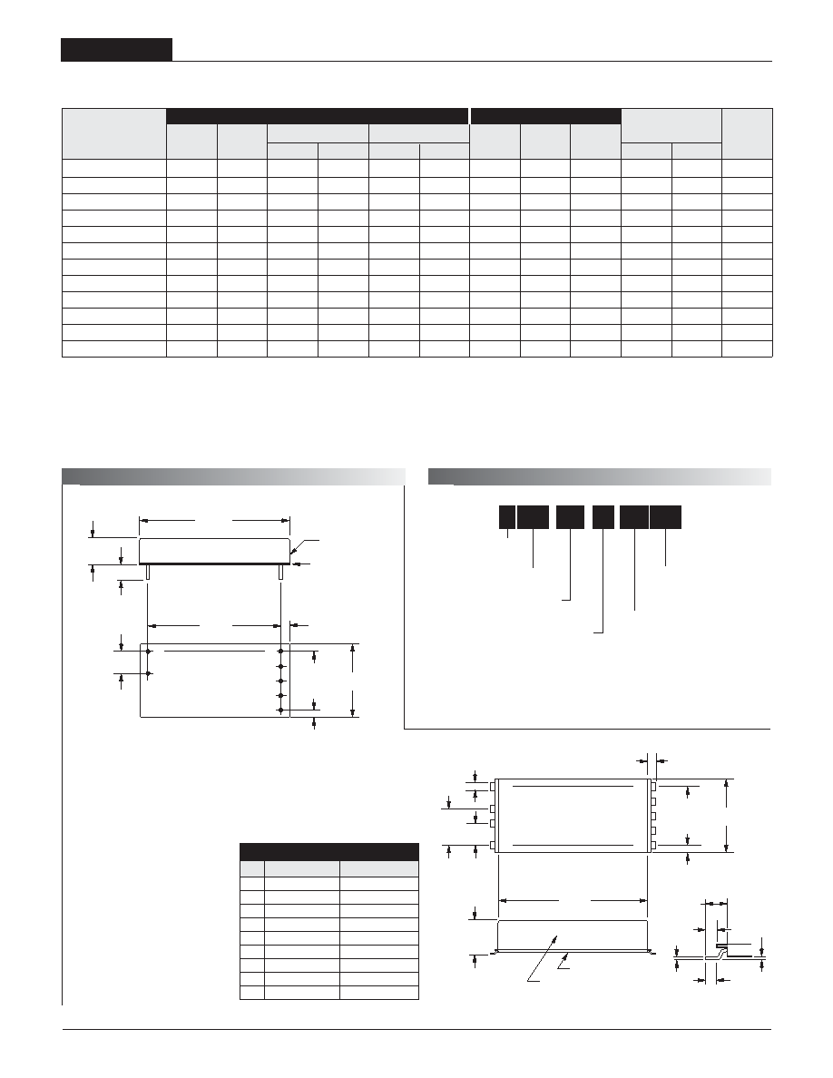
M E C H A N I C A L S P E C I F I C A T I O N S
2.00
(50.80)
4
3
2
1
8
7
6
5
9
0.10
(2.54)
0.110
(2.79)
0.100
(2.54)
0.300
(7.62)
0.500
(12.70)
TOP VIEW
1.00
(25.40)
0.800
(20.32)
4 EQ. SP. @
0.200 (5.08)
0.060
(1.52)
0.055
(1.40)
0.015
(0.38)
0.110
(2.79)
0.015
(0.38)
0.43
(10.92)
DIMENSIONS ARE IN INCHES (MM)
INSULATED BASE
METAL CASE
Case C18
Performance Specications and Ordering Guide
Output
Input
Non-Isolated
Output Conguration:
U = Unipolar
Nominal Output Voltage:
1.8, 2.5 or 3.3 Volts
Maximum Rated Output
Current in Amps
Input Voltage Range:
D5 = 4.75 to 5.5 Volts (5V nominal)
D12 = 10.8 to 13.6 Volts (12V nominal)
U NR
10
-
/
D5 SM
-
1.8
Packaging:
T = Through-Hole Package
SM = Surface-Mount Package
2
Package
VOUT
IOUT
R/N (mVp-p)
Regulation (Max.)
VIN Nom.
Range
IIN
Efciency
(Case,
Model
(Volts)
(Amps)
Typ.
Max.
Line
Load
(Volts)
(mA/mA)
Min.
Typ.
Pinout)
UNR-1.8/10-D5T
1.8
10
70
100
±0.1%
±0.5%
5
4.75-5.5
150/4190
82%
86%
C16A2, P23
UNR-1.8/10-D5SM
1.8
10
40
80
±0.1%
±0.5%
5
4.75-5.5
150/4190
82%
86%
C18, P25
UNR-2.5/10-D5T
2.5
10
75
100
±0.1%
±0.5%
5
4.75-5.5
150/5620
85%
89%
C16A2, P23
UNR-2.5/10-D5SM
2.5
10
75
100
±0.1%
±0.5%
5
4.75-5.5
150/5620
85%
89%
C18, P25
UNR-3.3/8-D5T
3.3
8
40
80
±0.1%
±0.5%
5
4.75-5.5
100/5470
88%
92%
C16A1, P23
UNR-3.3/8-D5SM
3.3
8
40
80
±0.1%
±0.5%
5
4.75-5.5
100/5470
88%
92%
C18, P25
UNR-3.3/8-D12T
3.3
8
40
100
±0.25%
±0.875%
12
10.8-13.6
50/2420
86%
91%
C16A1, P23
UNR-3.3/8-D12SM
3.3
8
40
100
±0.25%
±0.875%
12
10.8-13.6
50/2420
86%
91%
C18, P25
UNR-3.3/10-D5T
3.3
10
40
80
±0.1%
±0.5%
5
4.75-5.5
150/7250
86%
91%
C16A2, P23
UNR-3.3/10-D5SM
3.3
10
50
100
±0.1%
±0.5%
5
4.75-5.5
150/7250
86%
91%
C18, P25
UNR-3.3/10-D12T
3.3
10
70
120
±0.25%
±0.875%
12
10.8-13.6
90/3090
86%
89%
C16C2, P23
UNR-3.3/10-D12SM
3.3
10
70
120
±0.25%
±0.875%
12
10.8-13.6
90/3090
86%
89%
C18, P25
I/O Connections
Pin
Function P23
Function P25
1
Logic Ground
2
On/Off Control
3
+Output
N.C.
4
Trim
N.C.
5
Output Return
+Output
6
Input Return
Trim
7
+Input
Output Return
8
No Pin
Input Return
9
No Pin
+Input
Typical at TA = +25°C under nominal line voltage and full-load conditions, unless otherwise
noted. All models are tested and specied with an external 22F output capacitor
with a 200m
ESR and a 470F input capacitor with 6Arms ripple-current rating and 20m
ESR. See I/O Filtering and Noise Reduction for more details.
Ripple/Noise (R/N) is tested/specied over a 20MHz bandwidth. Output noise may be further
reduced by installing additional external output caps. See I/O Filtering and Noise Reduction.
These devices have no minimum-load requirements and will regulate under no-load conditions.
Nominal line voltage, no-load/full-load conditions.
0.10
(2.54)
METAL CASE
2.00
(50.80)
0.20 MIN
(5.08)
SEE
NOTES
INSULATED BASE
1
2
3
4
6
7
5
1.800
(45.72)
0.10
(2.54)
0.300
(7.62)
BOTTOM VIEW
DIMENSIONS IN INCHES (MM)
1.00
(25.40)
0.800
(20.32)
4 EQ. SP. @
0.200 (5.08)
0.10
(2.54)
CASE C16A1
CASE HEIGHT: 0.39 (9.91)
PIN DIAMETERS:
PINS 1-7:
0.040 ±0.002 (1.016 ±0.051)
CASE C16A2
CASE HEIGHT: 0.39 (9.91)
PIN DIAMETERS:
PINS 1-2, 4:
0.040 ±0.002 (1.016 ±0.051)
PINS 3, 5-7:
0.062 ±0.002 (1.575 ±0.051)
CASE C16C2
CASE HEIGHT: 0.48 (12.19)
PIN DIAMETERS:
PINS 1-2, 4:
0.040 ±0.002 (1.016 ±0.051)
PINS 3, 5-7:
0.062 ±0.002 (1.575 ±0.051)
Case C16A1, A2,C2
P A R T N U M B E R S T R U C T U R E
相關(guān)PDF資料 |
PDF描述 |
|---|---|
| UNR5112(UN5112) | Composite Device - Transistors with built-in Resistor |
| UNR5113(UN5113) | Composite Device - Transistors with built-in Resistor |
| UNR5114(UN5114) | Composite Device - Transistors with built-in Resistor |
| UNR5115(UN5115) | Composite Device - Transistors with built-in Resistor |
| UNR511M(UN511M) | 複合デバイス - 抵抗內(nèi)蔵型トランジスタ |
相關(guān)代理商/技術(shù)參數(shù) |
參數(shù)描述 |
|---|---|
| UNR4110 | 制造商:PANASONIC 制造商全稱:Panasonic Semiconductor 功能描述:Silicon PNP epitaxial planar type |
| UNR4110(UN4110) | 制造商:未知廠家 制造商全稱:未知廠家 功能描述:Composite Device - Transistors with built-in Resistor |
| UNR4110Q | 制造商:未知廠家 制造商全稱:未知廠家 功能描述:TRANSISTOR | 50V V(BR)CEO | 100MA I(C) | SPAK |
| UNR4110R | 制造商:未知廠家 制造商全稱:未知廠家 功能描述:TRANSISTOR | 50V V(BR)CEO | 100MA I(C) | SPAK |
發(fā)布緊急采購,3分鐘左右您將得到回復。