- 您現(xiàn)在的位置:買賣IC網(wǎng) > PDF目錄272835 > TXS100ZY-P2 (POWER-ONE INC) 1-OUTPUT 120 W DC-DC REG PWR SUPPLY MODULE PDF資料下載
參數(shù)資料
| 型號: | TXS100ZY-P2 |
| 廠商: | POWER-ONE INC |
| 元件分類: | 電源模塊 |
| 英文描述: | 1-OUTPUT 120 W DC-DC REG PWR SUPPLY MODULE |
| 封裝: | 2.400 X 3.450 INCH, 0.500 INCH HEIGHT, 3/4 BRICK PACKAGE-14 |
| 文件頁數(shù): | 15/27頁 |
| 文件大?。?/td> | 2635K |
| 代理商: | TXS100ZY-P2 |
第1頁第2頁第3頁第4頁第5頁第6頁第7頁第8頁第9頁第10頁第11頁第12頁第13頁第14頁當前第15頁第16頁第17頁第18頁第19頁第20頁第21頁第22頁第23頁第24頁第25頁第26頁第27頁
Product Specification
TXS Series: 75…120 A DC-DC Converters
36 to 75 V DC Input, 1.2, 1.5, 1.8, 2.0 and 2.5 V Output, 90 W to 250 W
REV. FEB 18, 2003
22 of 27
www.power-one.com
Radiated Noise
The radiated noise from the converter is extremely
difficult to predict since it depends largely upon the
motherboard
layout
and
the
switching
characteristic of the loads.
The report: “TXS layout considerations” on the
TXS product CD ROM provides recommendations
for reducing the radiated noise through shielding
and optimal layout.
Input Impedance
All switching power supplies exhibit negative input
impedance. A power source with inductive output
impedance and/or the wiring inductance from the
supply to the converter can affect the stability of
the modules.
A good general stability rule is, that the magnitude
of the source impedance should be lower than the
magnitude of the input impedance of the module at
all frequencies up to the switching frequency. The
minimum input impedance of a module is
calculated as 20 log(Ui min / Ii max).
Example: At Ui min = 36 V and Ii max = 7.8 A (see
Table 1 on page 3), a TXS100ZD needs an AC-
impedance
|Zline| < 13.2 dB at full load.
A possibility to reduce the input impedance is to
connect a low ESR input filter capacitor between
the input lines (at least 100 uF per 125 W output
power is recommended). With such a blocking
capacitor, a performance within the specifications
can be achieved with almost all supply conditions.
To consider:
- The stabilising input capacitor and the capacitors
of the input filters generate an inrush current.
- The blocking capacitor should be able to handle
the input ripple current of the module, which is
much larger than the reflected input ripple (see
measurement set up: figures 20/22).
- The capacitors may resonate with the inductance
of the input filter and the wiring. If this happens,
the resonance will require damping.
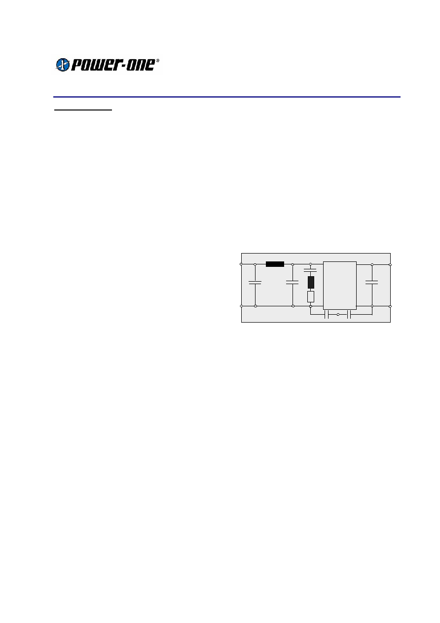
On Board Input and Output Filters
TXS converters use a topology that achieves input-
and output ripple frequencies four times higher
than the switching frequency. This results in
excellent ripple and noise values and low external
filter requirements.
The on board output filter is a parallel connection
of very low impedance Tantalum capacitors
connected in parallel with an overall capacitance of
3.3 mF. Total ESR < 4.5 m
(@100 kHz/25 °C).
The high efficient on-board input filter consists of
several ceramic capacitors, a damping network
and a filter inductor. Two EMC capacitors
(Cy1+Cy2) in a series connection with 2.2 nF
each, are connected between primary and
secondary.
Lin
C1
C2
TXS
pow er s t age
C3
1
2
5
6
Cy 1 + C y 2
Figure 52: On board input and output filters.
C1 =1uF, C2 =6 (1 uF), C3 =3 mF
Cy = 1.1 nF,
Lin = 0.9 uH
for
TXS
models ZC and ZD, 1.1 uH for models
ZY, ZA and ZB
Electromagnetic Susceptibility
The converter does not react to EMI pulses.
However the Y capacitors and the interwinding
capacitance of the multilayer board can couple
some common mode noise to the secondary.
Earthing or decoupling the output with large Y
capacitors needs a two stage EMC filter or a
ground line inductor to meet the EMC conducted
noise level B (see EMC specifications).
-
The EMI measurements have been done with
a one stage input filter according to Figure 44.
-
ESD pulses were directly discharged into the
TXS pins.
-
Burst pulses were applied in front of the input
filter.
Performance criterion A denotes normal operation,
no deviation from specification. Performance
criterion B denotes temporary deviation from
specification.
相關PDF資料 |
PDF描述 |
|---|---|
| TXS120ZA-N2V | 1-OUTPUT 180 W DC-DC REG PWR SUPPLY MODULE |
| TXS120ZA-R3H | 1-OUTPUT 180 W DC-DC REG PWR SUPPLY MODULE |
| TXS120ZY-P21V | 1-OUTPUT 144 W DC-DC REG PWR SUPPLY MODULE |
| TXS75ZY-P2R2V | 1-OUTPUT 90 W DC-DC REG PWR SUPPLY MODULE |
| TXS80ZD-3V | 1-OUTPUT 200 W DC-DC REG PWR SUPPLY MODULE |
相關代理商/技術參數(shù) |
參數(shù)描述 |
|---|---|
| TXS10AU08AI | 制造商:TE Connectivity 功能描述: |
| TXS10AU12AI | 功能描述:環(huán)形MIL規(guī)格應變消除裝置與適配器 ADAPTER: RoHS:否 制造商:Amphenol Industrial 產(chǎn)品:Cable Clamps 類型:Bushing Cable Clamps MIL 類型:MIL-DTL-5015 系列:97 外殼大小:16S, 16 匹配樣式:Threaded 主體材料:Aluminum Alloy 主體類型:Straight |
| TXS10P-100A | 制造商:TOPSTEK 制造商全稱:TOPSTEK 功能描述:Anti-Magnet AC Current Sensors |
| TXS18X | 制造商:YSTONE 制造商全稱:Yellow Stone Corp 功能描述:TAPED LED LAMP |
| TXS2-1.5V | 功能描述:低信號繼電器 - PCB 2 Form C 2A 30VDC 1.5VDC RoHS:否 制造商:NEC 觸點形式:2 Form C (DPDT-BM) 觸點電流額定值: 線圈電壓:5 V 最大開關電流:1 A 線圈電流:1 A 線圈類型:Non-Latching 功耗:140 mW 端接類型:SMT 絕緣: 介入損耗: |
發(fā)布緊急采購,3分鐘左右您將得到回復。