- 您現(xiàn)在的位置:買賣IC網(wǎng) > PDF目錄384032 > TVP3026-250 (Texas Instruments, Inc.) Video Interface PALETTE Exract(組合像素模式視頻接口調色器) PDF資料下載
參數(shù)資料
| 型號: | TVP3026-250 |
| 廠商: | Texas Instruments, Inc. |
| 英文描述: | Video Interface PALETTE Exract(組合像素模式視頻接口調色器) |
| 中文描述: | 視頻接口調色板Exract(組合像素模式視頻接口調色器) |
| 文件頁數(shù): | 38/107頁 |
| 文件大小: | 707K |
| 代理商: | TVP3026-250 |
第1頁第2頁第3頁第4頁第5頁第6頁第7頁第8頁第9頁第10頁第11頁第12頁第13頁第14頁第15頁第16頁第17頁第18頁第19頁第20頁第21頁第22頁第23頁第24頁第25頁第26頁第27頁第28頁第29頁第30頁第31頁第32頁第33頁第34頁第35頁第36頁第37頁當前第38頁第39頁第40頁第41頁第42頁第43頁第44頁第45頁第46頁第47頁第48頁第49頁第50頁第51頁第52頁第53頁第54頁第55頁第56頁第57頁第58頁第59頁第60頁第61頁第62頁第63頁第64頁第65頁第66頁第67頁第68頁第69頁第70頁第71頁第72頁第73頁第74頁第75頁第76頁第77頁第78頁第79頁第80頁第81頁第82頁第83頁第84頁第85頁第86頁第87頁第88頁第89頁第90頁第91頁第92頁第93頁第94頁第95頁第96頁第97頁第98頁第99頁第100頁第101頁第102頁第103頁第104頁第105頁第106頁第107頁
2–24
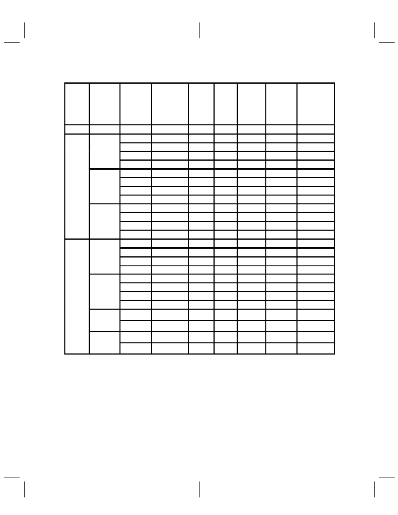
Table 2–17. Multiplex Mode and Bus-Width Selection
MODE
SUB-
MODE
TRUE-
COLOR-
CONTROL
REGISTER
(INDEX
0x18)
MULTIPLEX-
CONTROL
REGISTER
(INDEX
0x19)
DATA
BITS
PER
PIXEL
(see
Note 3)
PIXEL
BUS
WIDTH
MULTI-
PLEX
RATIO
(see
Note 4)
OVERLAY
BITS
PER
PIXEL
TABLE
REFERENCE
(see
Note 5)
VGA
0x80
0x98
8
8
1
NA
v1
Pseud
Color
d
1
0x80
0x41
4
8
2
NA
s1
4-Bit,
Normal
0x80
0x42
4
16
4
NA
s2
0x80
0x43
4
32
8
NA
s3
0x80
0x44
4
64
16
NA
s4
2
0x80
0x61
4
8
2
NA
s5
4-Bit,
4 Bit,
Nibble
Swapped
0x80
0x62
4
16
4
NA
s6
0x80
0x63
4
32
8
NA
s7
0x80
0x64
4
64
16
NA
s8
3
0x80
0x49
8
8
1
NA
s9
0x80
0x4A
8
16
2
NA
s10
8-Bit
0x80
0x4B
8
32
4
NA
s11
0x80
0x4C
8
64
8
NA
s12
Direct-
Color
1
0x16
0x5B
24
32
4:3
NA
d1
Packed-24
Packed 24
R-G-B
8 8 8
8–8–8
0x16
0x5C
24
64
8:3
NA
d2
0x1E
0x5B
24
32
5:4
NA
d3
0x1E
0x5C
24
64
5:2
NA
d4
2
0x17
0x5B
24
32
4:3
NA
d5
Packed-24
Packed 24
B-G-R
8 8 8
8–8–8
0x17
0x5C
24
64
8:3
NA
d6
0x1F
0x5B
24
32
5:4
NA
d7
0x1F
0x5C
24
64
5:2
NA
d8
3
32-Bit
O-R-G-B
0x06
0x5B
24
32
1
8
d9
0x06
0x5C
24
64
2
8
d10
4
32-bit
B-G-R-O
0x07
0x5B
24
32
1
8
d11
0x07
0x5C
24
64
2
8
d12
NOTES:
3. Data bits per pixel is the number of bits of pixel information used as color data for each displayed pixel, often
referred to as the number of bit planes.
4. Multiplex ratio indicates the number of pixels per bus load or the number of pixels associated with each
LCLK (load clock) pulse. For example, with a 64-bit pixel bus width and 8 bit planes, each bus load is
comprised of 8 pixels. The RCLK frequency must be chosen as a function of the multiplex mode selected.
The RCLK frequency is not automatically set by mode selection; it must be set by programming the loop
clock PLL registers.
5. This column is a reference to Tables 2–18 through 2–21, where the actual manipulation of pixel information
and pixel latching sequences are illustrated for each of the multiplexing modes. For the pseudo-color pixel
latching sequence (V1 and S1 through S12) refer to Table 2–18. For the packed-24 mode pixel latching
sequence associated with the direct-color and true-color modes, refer to Table 2–19. For the direct-color
mode pixel latching sequence, refer to Table 2–20 for little-endian format and to Table 2–21 for big-endian
format.
相關PDF資料 |
PDF描述 |
|---|---|
| TX24 | 60.8 MM 5 X 8 DOT MATRIX DISPLAYS |
| TXB0102DCTR | 2-BIT BIDIRECTIONAL VOLTAGE-LEVEL TRANSLATOR WITH AUTO DIRECTION SENSING AND 【15-kV ESD PROTECTION |
| TXB0102DCTT | 2-BIT BIDIRECTIONAL VOLTAGE-LEVEL TRANSLATOR WITH AUTO DIRECTION SENSING AND 【15-kV ESD PROTECTION |
| TZX7V5D | surface mount silicon Zener diodes |
| TZX6V2 | surface mount silicon Zener diodes |
相關代理商/技術參數(shù) |
參數(shù)描述 |
|---|---|
| TVP3026-250AMDN | 制造商:TI 制造商全稱:Texas Instruments 功能描述:Video Interface Palette |
| TVP3026-250APCE | 制造商:TI 制造商全稱:Texas Instruments 功能描述:Video Interface Palette |
| TVP3026-250BMDN | 制造商:TI 制造商全稱:Texas Instruments 功能描述:Video Interface Palette |
| TVP3026-250BPCE | 制造商:Rochester Electronics LLC 功能描述:- Bulk 制造商:Texas Instruments 功能描述: |
| TVP3026-250CPCE | 制造商:Rochester Electronics LLC 功能描述:- Bulk |
發(fā)布緊急采購,3分鐘左右您將得到回復。