- 您現(xiàn)在的位置:買賣IC網(wǎng) > PDF目錄371188 > TSA5059 (NXP Semiconductors N.V.) 2.7 GHz I2C-bus controlled low phase noise frequency synthesizer PDF資料下載
參數(shù)資料
| 型號(hào): | TSA5059 |
| 廠商: | NXP Semiconductors N.V. |
| 英文描述: | 2.7 GHz I2C-bus controlled low phase noise frequency synthesizer |
| 中文描述: | 2.7千兆赫的I2C控制的低相位噪聲頻率合成器總線 |
| 文件頁(yè)數(shù): | 8/24頁(yè) |
| 文件大小: | 151K |
| 代理商: | TSA5059 |
第1頁(yè)第2頁(yè)第3頁(yè)第4頁(yè)第5頁(yè)第6頁(yè)第7頁(yè)當(dāng)前第8頁(yè)第9頁(yè)第10頁(yè)第11頁(yè)第12頁(yè)第13頁(yè)第14頁(yè)第15頁(yè)第16頁(yè)第17頁(yè)第18頁(yè)第19頁(yè)第20頁(yè)第21頁(yè)第22頁(yè)第23頁(yè)第24頁(yè)

1999 Oct 05
8
Philips Semiconductors
Preliminary specification
2.7 GHz I
2
C-bus controlled low phase
noise frequency synthesizer
TSA5059
READ mode: R/W = 1
Data can be read out of the TSA5059 by setting the
bit R/W to logic 1 (see Table 5). After the slave address
has been recognized, the TSA5059 generates an
acknowledge pulse and the first data byte (status word) is
transferredontheSDA line(MSBfirst).Dataisvalidonthe
SDA line during a HIGH-level of the SCL clock signal.
A second data byte can be read out of the TSA5059 if the
controller generates an acknowledge on the SDA line.
End of transmission will occur if no acknowledge from the
controller occurs.The TSA5059 will then release the data
line to allow the controller to generate a STOP condition.
When ports P0 to P2 are used as inputs, they must be
programmed in their high-impedance state.
The POR flag is set to logic 1 when V
CC
drops below
approximately 2.75 V and at power-on.
It is reset to logic 0 when an end of data is detected by the
TSA5059 (end of a READ sequence).
Control of the loop is made possible with the in-lock flag
which indicates (bit FL = 1) when the loop is phase-locked.
The bits I2, I1 and I0 represent the status of the I/O ports
P2, P1 and P0 respectively. A logic 0 indicates a
LOW-level and a logic 1 indicates a HIGH-level.
A built-in 5-level ADC is available at pin ADC. This
converter can be used to feed AFC information to the
microcontroller through the I
2
C-bus. The relationship
between bits A2, A1, A0 and the input voltage at pin ADC
is given in Table 7.
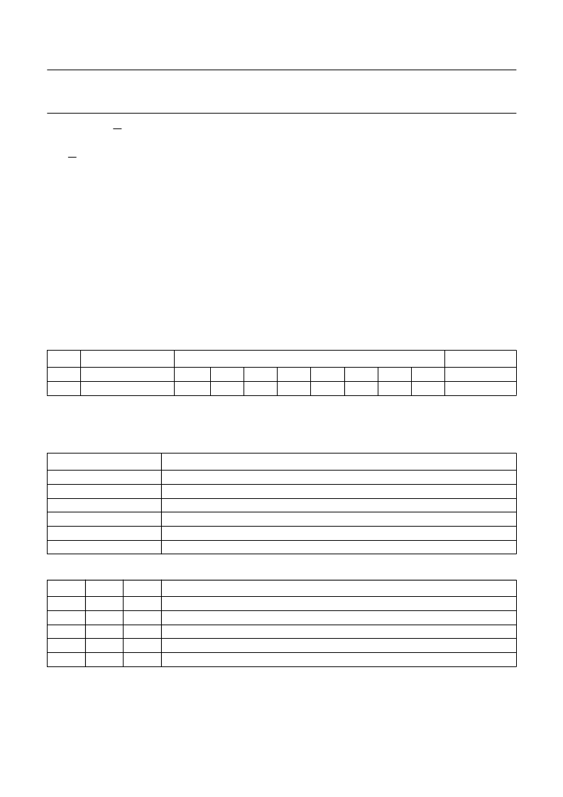
Table 5
Read data format
Note
1.
MSB is transmitted first.
Table 6
Explanation of Table 5
Table 7
ADC levels
Note
1.
Accuracy is
±
0.03V
CC
.
BYTE
DESCRIPTION
MSB
(1)
LSB
CONTROL BIT
1
2
address
status byte
1
1
0
I2
0
I1
0
I0
MA1
A2
MA0
A1
1
A
POR
FL
A0
BIT
DESCRIPTION
A
MA1 and MA0
POR
FL
I2, I1 and I0
A2, A1 and A0
acknowledge bit
programmable address bits; see Table 3
Power-on reset flag (bit POR = 1 on power-on)
in-lock flag (bit FL = 1 when the loop is phase-locked)
digital information for I/O ports P2, P1 and P0 respectively
digital outputs of the 5-level ADC; see Table 7
A2
A1
A0
VOLTAGE APPLIED TO PIN ADC
(1)
1
0
0
0
0
0
1
1
0
0
0
1
0
1
0
0.6V
CC
to V
CC
0.45V
CC
to 0.6V
CC
0.3V
CC
to 0.45V
CC
0.15V
CC
to 0.3V
CC
0 to 0.15V
CC
相關(guān)PDF資料 |
PDF描述 |
|---|---|
| TSA5059T | 2.7 GHz I2C-bus controlled low phase noise frequency synthesizer |
| TSC2200 | PDA ANALOG INTERFACE CIRCUIT |
| TSC2200IPW | PDA ANALOG INTERFACE CIRCUIT |
| TSC2200IPWR | PDA ANALOG INTERFACE CIRCUIT |
| TSC2200IRHB | PDA ANALOG INTERFACE CIRCUIT |
相關(guān)代理商/技術(shù)參數(shù) |
參數(shù)描述 |
|---|---|
| TSA5059A | 制造商:PHILIPS 制造商全稱:NXP Semiconductors 功能描述:2.7 GHz I2C-bus controlled low phase noise frequency synthesizer |
| TSA5059AT | 制造商:PHILIPS 制造商全稱:NXP Semiconductors 功能描述:2.7 GHz I2C-bus controlled low phase noise frequency synthesizer |
| TSA5059AT/C2,518 | 制造商:NXP Semiconductors 功能描述: |
| TSA5059ATS | 制造商:PHILIPS 制造商全稱:NXP Semiconductors 功能描述:2.7 GHz I2C-bus controlled low phase noise frequency synthesizer |
| TSA5059ATS/C1,118 | 功能描述:鎖相環(huán) - PLL 2,7GHZI2C BUS RoHS:否 制造商:Silicon Labs 類型:PLL Clock Multiplier 電路數(shù)量:1 最大輸入頻率:710 MHz 最小輸入頻率:0.002 MHz 輸出頻率范圍:0.002 MHz to 808 MHz 電源電壓-最大:3.63 V 電源電壓-最小:1.71 V 最大工作溫度:+ 85 C 最小工作溫度:- 40 C 封裝 / 箱體:QFN-36 封裝:Tray |
發(fā)布緊急采購(gòu),3分鐘左右您將得到回復(fù)。