- 您現(xiàn)在的位置:買賣IC網(wǎng) > PDF目錄383961 > TMX320DM6437BZDUA (Texas Instruments, Inc.) Digital Media Processor PDF資料下載
參數(shù)資料
| 型號: | TMX320DM6437BZDUA |
| 廠商: | Texas Instruments, Inc. |
| 英文描述: | Digital Media Processor |
| 中文描述: | 數(shù)字媒體處理器 |
| 文件頁數(shù): | 110/309頁 |
| 文件大小: | 2216K |
| 代理商: | TMX320DM6437BZDUA |
第1頁第2頁第3頁第4頁第5頁第6頁第7頁第8頁第9頁第10頁第11頁第12頁第13頁第14頁第15頁第16頁第17頁第18頁第19頁第20頁第21頁第22頁第23頁第24頁第25頁第26頁第27頁第28頁第29頁第30頁第31頁第32頁第33頁第34頁第35頁第36頁第37頁第38頁第39頁第40頁第41頁第42頁第43頁第44頁第45頁第46頁第47頁第48頁第49頁第50頁第51頁第52頁第53頁第54頁第55頁第56頁第57頁第58頁第59頁第60頁第61頁第62頁第63頁第64頁第65頁第66頁第67頁第68頁第69頁第70頁第71頁第72頁第73頁第74頁第75頁第76頁第77頁第78頁第79頁第80頁第81頁第82頁第83頁第84頁第85頁第86頁第87頁第88頁第89頁第90頁第91頁第92頁第93頁第94頁第95頁第96頁第97頁第98頁第99頁第100頁第101頁第102頁第103頁第104頁第105頁第106頁第107頁第108頁第109頁當(dāng)前第110頁第111頁第112頁第113頁第114頁第115頁第116頁第117頁第118頁第119頁第120頁第121頁第122頁第123頁第124頁第125頁第126頁第127頁第128頁第129頁第130頁第131頁第132頁第133頁第134頁第135頁第136頁第137頁第138頁第139頁第140頁第141頁第142頁第143頁第144頁第145頁第146頁第147頁第148頁第149頁第150頁第151頁第152頁第153頁第154頁第155頁第156頁第157頁第158頁第159頁第160頁第161頁第162頁第163頁第164頁第165頁第166頁第167頁第168頁第169頁第170頁第171頁第172頁第173頁第174頁第175頁第176頁第177頁第178頁第179頁第180頁第181頁第182頁第183頁第184頁第185頁第186頁第187頁第188頁第189頁第190頁第191頁第192頁第193頁第194頁第195頁第196頁第197頁第198頁第199頁第200頁第201頁第202頁第203頁第204頁第205頁第206頁第207頁第208頁第209頁第210頁第211頁第212頁第213頁第214頁第215頁第216頁第217頁第218頁第219頁第220頁第221頁第222頁第223頁第224頁第225頁第226頁第227頁第228頁第229頁第230頁第231頁第232頁第233頁第234頁第235頁第236頁第237頁第238頁第239頁第240頁第241頁第242頁第243頁第244頁第245頁第246頁第247頁第248頁第249頁第250頁第251頁第252頁第253頁第254頁第255頁第256頁第257頁第258頁第259頁第260頁第261頁第262頁第263頁第264頁第265頁第266頁第267頁第268頁第269頁第270頁第271頁第272頁第273頁第274頁第275頁第276頁第277頁第278頁第279頁第280頁第281頁第282頁第283頁第284頁第285頁第286頁第287頁第288頁第289頁第290頁第291頁第292頁第293頁第294頁第295頁第296頁第297頁第298頁第299頁第300頁第301頁第302頁第303頁第304頁第305頁第306頁第307頁第308頁第309頁
www.ti.com
P
TMS320DM6437
Digital Media Processor
SPRS345B–NOVEMBER 2006–REVISED MARCH 2007
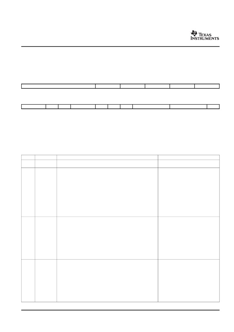
3.7.2.2
PINMUX1 Register Description
The Pin Multiplexing 1 Register (PINMUX1) controls the pin multiplexing of all Pin Mux Blocks. The
PINMUX1 register format is shown in
Figure 3-13
and the bit field descriptions are given in
Table 3-20
.
Some muxed pins are controlled by more than one PINMUX bit field. For the combination of PINMUX bit
fields that control each muxed pin, see
Section 3.7.3.1
,
Multiplexed Pins on DM6437
.
31
26
25
24
23
22
21
20
19
18
17
16
RESERVED
SPBK1
SPBK0
TIM1BK
RSV
TIM0BK
R/W-0000 00
R/W-00
R/W-00
R/W-00
R/W-00
R/W-00
15
14
13
12
11
10
9
8
7
6
5
4
3
2
1
0
CKOBK
RSV
PWM1BK
UR0FCBK
RSV
UR0DBK
RSV
HOSTBK
RESERVED
PCIEN
R/W-01
R/W-0
R/W-0
R/W-00
R/W-0
R/W-0
R/W-0
R/W-000
R/W-000
R-P
LEGEND: R/W = Read/Write; R = Read only; P = specified pin state; -
n
= value after reset
(1)
For proper DM6437 device operation,
always
write a value of "0" to all RESERVED/RSV bits.
Figure 3-13. PINMUX1 Register
(1)
Table 3-20. PINMUX1 Register Bit Descriptions
Bit
Field Name
Description
Pins Controlled
Reserved. For proper device operation, the user should only write "0" to this bit
(
default
).
31:26
RESERVED
–
Serial Port Sub-Block 1 Pin Select.
Selects the function of the multiplexed pins in the Serial Port Sub-Block 1.
00 = GPIO Mode (
default
).
Pins function as GPIO (GP[110:105]).
Serial Port Sub-Block 1:
AXR0[0]/FSR1/GP[105]
ACLKX0/CLKX1/GP[106]
AFSX0/DX1/GP[107]
AHCLKX0/CLKR1/GP[108]
AMUTEIN0/FSX1/GP[109]
AMUTE0/DR1/GP[110]
01 = McBSP1 Mode.
Pins function as McBSP1: CLKX1, FSX1, DX1, CLKR1, FSR1, and DR1.
25:24
SPBK1
10 = McASP0 Transmit and 1 serializer.
Pins function as McASP0: AXR0[0], ACLKX0, AFSX0, AHCLKX0, AMUTEIN0,
and AMUTE0.
11 = McBSP1 Transmit + McASP0 SPDIF Mode.
Pins function as McBSP1 transmit (CLKX1, FSX1, DX1)
and
McASP0 SPDIF
(AXR0[0], AHCLKX0, AMUTE0).
Serial Port Sub-Block 0 Pin Select.
Selects the function of the multiplexed pins in the Serial Port Sub-Block 0.
00 = GPIO Mode (
default
).
Pins function as GPIO (GP[104:99]).
Serial Port Sub-Block 0:
ACLKR0/CLKX0/GP[99]
AFSR0/DR0/GP[100]
AHCLKR0/CLKR0/GP[101]
AXR0[3]/FSR0/GP[102]
AXR0[2]/FSX0/GP[103]
AXR0[1]/DX0/GP[104]
01 = McBSP0 Mode.
Pins function as McBSP0 CLKX0, FSX0, DX0, CLKR0, FSR0, and DR0.
23:22
SPBK0
10 = McASP0 Receive and 3 serializers.
Pins function as McASP0 ACLKR0, AFSR0, AHCLKR0, AXR0_3, AXR0_2, and
AXR0_1.
11 = Reserved
Timer1 Block Pin Select.
Selects the function of the multiplexed pins in theTimer1 Block.
00 = GPIO Mode (
default
).
Pins function as GPIO (GP[56:55]).
Timer1 Block:
HECC_RX/TINP1L/URXD1/GP[56]
HECC_TX/TOUT1L/UTXD1/GP[55]
01 = Timer1 Mode.
Pins function as Timer1 TINP1L and TOUT1L.
21:20
TIM1BK
10 = UART1 Data Mode.
Pins function as UART1 data pins URXD1 and UTXD1.
11 = HECC Mode.
Pins function as HECC HECC_RX and HECC_TX.
Device Configurations
110
Submit Documentation Feedback
相關(guān)PDF資料 |
PDF描述 |
|---|---|
| TMX320DM6437BZWTA | Digital Media Processor |
| TMS320DM6443_07 | Digital Media System-on-Chip |
| TMX320DM6443AZWT | Digital Media System-on-Chip |
| TMX320DM6443ZWT | Digital Media System-on-Chip |
| TMS320DM647_08 | Digital Media Processor |
相關(guān)代理商/技術(shù)參數(shù) |
參數(shù)描述 |
|---|---|
| TMX320DM6437BZWTA | 功能描述:數(shù)字信號處理器和控制器 - DSP, DSC Dig Media Processor RoHS:否 制造商:Microchip Technology 核心:dsPIC 數(shù)據(jù)總線寬度:16 bit 程序存儲器大小:16 KB 數(shù)據(jù) RAM 大小:2 KB 最大時鐘頻率:40 MHz 可編程輸入/輸出端數(shù)量:35 定時器數(shù)量:3 設(shè)備每秒兆指令數(shù):50 MIPs 工作電源電壓:3.3 V 最大工作溫度:+ 85 C 封裝 / 箱體:TQFP-44 安裝風(fēng)格:SMD/SMT |
| TMX320DM6441CZWT | 制造商:Texas Instruments 功能描述: |
| TMX320DM6441DZWT | 制造商:Texas Instruments 功能描述:DAVINCI DIGITAL MEDIA SYSTEM-ON-CHIP - Tape and Reel |
| TMX320DM6443AZWT | 制造商:Rochester Electronics LLC 功能描述:DAVINCI DIGITAL MEDIA SYSTEM-ON-CHIP - Tape and Reel |
| TMX320DM6443BZWT | 制造商:Texas Instruments 功能描述: |
發(fā)布緊急采購,3分鐘左右您將得到回復(fù)。