- 您現(xiàn)在的位置:買賣IC網(wǎng) > PDF目錄371182 > TDA8020 (NXP Semiconductors N.V.) Dual smart card interface PDF資料下載
參數(shù)資料
| 型號(hào): | TDA8020 |
| 廠商: | NXP Semiconductors N.V. |
| 英文描述: | Dual smart card interface |
| 中文描述: | 雙界面智能卡 |
| 文件頁數(shù): | 10/24頁 |
| 文件大小: | 114K |
| 代理商: | TDA8020 |

2001 Aug 15
10
Philips Semiconductors
Product specification
Dual smart card interface
TDA8020HL
If a start bit is detected on the I/O during the first 200 CLK
pulses, then it is omitted. If a start bit is detected between
200 and 352 CLK pulses, then bit EARLY is set in the
status register. If the card starts answering before
41950 CLK pulses, then RST remains LOW level. If not,
after 41950 CLK pulses, RST is toggled HIGH. If, again, a
start bit is detected within 352 CLK pulses, bit EARLY is
set in the status register. If the card does not answer
before 41950 new CLK pulses, then bit MUTE is set in the
status register. If the card answers within the correct
window, then the CLK count is stopped and the system
controller may send commands to the card.
Deactivation is initiated either by the system controller
(reset bit START), or automatically in the event of a
hardware problem or supply drop-out. With a supply
drop-out both cards are deactivated at the same time.
During deactivation, RST goes LOW, the clock is stopped
and the I/O lines go LOW. V
CC
then goes low with a
controlled slope and the DC/DC converter is stopped if no
card is active.
Outside a session, cards contacts are forced low
impedance to CGND.
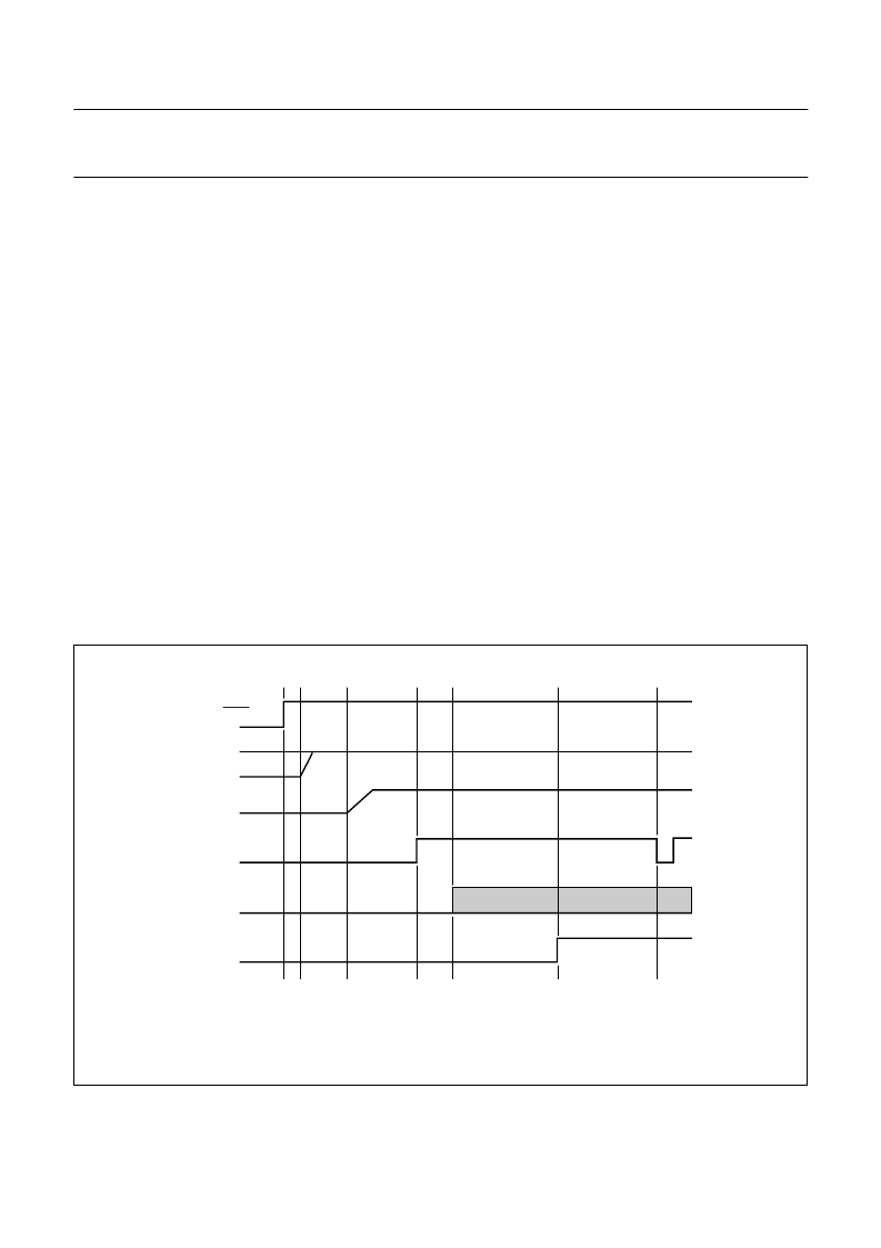
Activation sequence
When the cards are inactive, V
CC
, CLK, RST and I/O are
LOW, with low impedance with respect to CGND. The
DC/DC converter is stopped.
When everything is satisfactory (voltage supply, card
present and no hardware problems), the system controller
may initiate an activation sequence of a present card
(see Fig.4):
The DC/DC converter is started (t1). If one card was
already active, then the DC/DC converter was already
on, and nothing more occurs at this step
V
CC
starts rising from 0 to 5 or 3 V with a controlled rise
time of 0.14 V/
μ
s typical (t2)
I/O rises to V
CC
(t3); internal 10 k
pull-up resistors to
V
CC
CLK is sent to the card and RST is enabled (t4 = t
act
).
If the card does not answer within the first 41950 CLK
cycles, then RST is raised HIGH (t5).
The sequencer is clocked by f
int
/64 which leads to a time
interval T of 25
μ
s typical. Thus t1 = 0 to T/64;
t2 = t1 + 3T/2; t3 = t1 + 7T/2 and t4 = t1 + 4T.
VUP
VCC
I/O
CLK
RST
handbook, full pagewidth
START/STOP
t0 t1
t2
t3
t4
t5
FCE837
ATR
Fig.4 Activation sequence.
t4 = t
act
.
相關(guān)PDF資料 |
PDF描述 |
|---|---|
| TDA8260 | Satellite Zero-IF QPSK/8PSK downconverter with PLL synthesizer |
| TDA8260TW | Satellite Zero-IF QPSK/8PSK downconverter with PLL synthesizer |
| TDA8304 | SMALL SIGNAL COMBINATION IC FOR COLOUR TV |
| TDA8315 | Integrated NTSC decoder and sync processor |
| TDA8315T | Integrated NTSC decoder and sync processor |
相關(guān)代理商/技術(shù)參數(shù) |
參數(shù)描述 |
|---|---|
| TDA8020HL | 制造商:PHILIPS 制造商全稱:NXP Semiconductors 功能描述:Dual smart card interface |
| TDA8020HL/C1,118 | 功能描述:輸入/輸出控制器接口集成電路 SMART CARD INTERFACE RoHS:否 制造商:Silicon Labs 產(chǎn)品: 輸入/輸出端數(shù)量: 工作電源電壓: 最大工作溫度:+ 85 C 最小工作溫度:- 40 C 安裝風(fēng)格:SMD/SMT 封裝 / 箱體:QFN-64 封裝:Tray |
| TDA8020HL/C2 | 制造商:NXP Semiconductors 功能描述:Cut Tape |
| TDA8020HL/C2,118 | 功能描述:輸入/輸出控制器接口集成電路 SMART CARD INTERFACE DUAL RoHS:否 制造商:Silicon Labs 產(chǎn)品: 輸入/輸出端數(shù)量: 工作電源電壓: 最大工作溫度:+ 85 C 最小工作溫度:- 40 C 安裝風(fēng)格:SMD/SMT 封裝 / 箱體:QFN-64 封裝:Tray |
| TDA8020HL/C2,151 | 功能描述:接口 - 專用 Dual IC card interface RoHS:否 制造商:Texas Instruments 產(chǎn)品類型:1080p60 Image Sensor Receiver 工作電源電壓:1.8 V 電源電流:89 mA 最大功率耗散: 最大工作溫度:+ 85 C 安裝風(fēng)格:SMD/SMT 封裝 / 箱體:BGA-59 |
發(fā)布緊急采購,3分鐘左右您將得到回復(fù)。