- 您現(xiàn)在的位置:買賣IC網(wǎng) > PDF目錄373624 > TDA7546 (意法半導體) Multichip module for TMC tuner applications PDF資料下載
參數(shù)資料
| 型號: | TDA7546 |
| 廠商: | 意法半導體 |
| 英文描述: | Multichip module for TMC tuner applications |
| 中文描述: | 豐田汽車多芯片模塊調(diào)諧器應(yīng)用 |
| 文件頁數(shù): | 55/68頁 |
| 文件大小: | 823K |
| 代理商: | TDA7546 |
第1頁第2頁第3頁第4頁第5頁第6頁第7頁第8頁第9頁第10頁第11頁第12頁第13頁第14頁第15頁第16頁第17頁第18頁第19頁第20頁第21頁第22頁第23頁第24頁第25頁第26頁第27頁第28頁第29頁第30頁第31頁第32頁第33頁第34頁第35頁第36頁第37頁第38頁第39頁第40頁第41頁第42頁第43頁第44頁第45頁第46頁第47頁第48頁第49頁第50頁第51頁第52頁第53頁第54頁當前第55頁第56頁第57頁第58頁第59頁第60頁第61頁第62頁第63頁第64頁第65頁第66頁第67頁第68頁
TDA7546
Software specifications
55/68
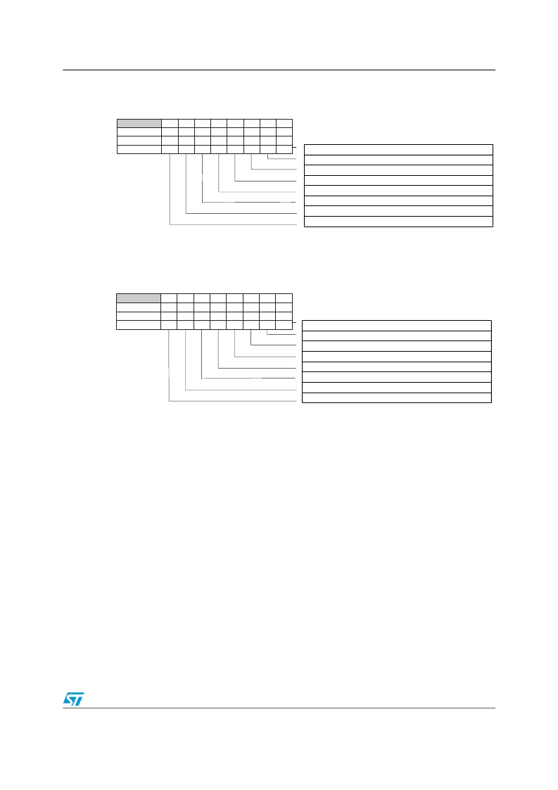
Table 48.
pllreg1 register
Table 49.
pllreg0 register
Note:
sinc4reg and testreg registers are dedicated for testing and are not described in this
specification.
Reset values of rds_qu, rds_corrp, rds_bd_h and rds_bd_l registers are not visible for the
programmer, because he can see only the copy of this registers in the RAM buffer after a
new RDS block was received.
The pllreg4-0 registers must be initialized first, before the RDS functionality can be used. If
the “PLLEN” bit of pllreg4 is set from zero to one, then the PLL will be initialized after
I
2
C/SPI transfer with the actual values of pllreg4-0. After the lock time the PLL switches
automatically over to the PLL output clock. The next I
2
C/SPI transfer is only allowed after the
lock time (500
μ
s) and additional 25 XTI input clock cycles. If the “PLLEN” bit is set from one
to zero, the PLL will be stopped and the system clock is switched back to the XTI input clock
(after the I
2
C/SPI transfer). The next I
2
C/SPI transfer is then only allowed after 25 XTI input
clock cycles. This is to avoid any I
2
C/SPI communication during clock switching.
The registers pllreg3-1 can be only changed at once. If there are less then all three pllreg3-
1 registers written during a I
2
C/SPI transfer, then they will be not updated.
If the XTI input frequency is 10.25MHz, then only register pllreg4 must be programmed,
because the pllreg3-0 register reset values can be used without any modification.
(10) Reset values are designed for 10.25 MHz XTI in-
put frequency.
(11) MF values smaller than 9 are ignored, 9 is then
used internally.
bit 8 of fractional factor (10) (12).
bit 9 of fractional factor (10) (12).
bit 10 of fractional factor (10) (12).
bit 11 of fractional factor (10) (12).
bit 12 of fractional factor (10) (12).
bit 13 of fractional factor (10) (12).
bit 0 of PLL multiplication factor (10) (11) (12).
bit 1 of PLL multiplication factor (10) (11) (12).
bit name
access
bit 7
bit 0
bit 1
bit 2
bit 3
bit 4
bit 5
bit 6
r/w
r/w
r/w
r/w
r/w
r/w
r/w
r/w
FRA8
FRA9
FRA12
MF1
FRA13
MF0
FRA11 FRA10
reset value
0
1
1
0
0
0
0
1
pllreg1
(12) The registers pllreg3, pllreg2 and pllreg1 must be
written at once to be updated, i.e. if the I2C/SPI stops
after pllreg2, then these registers are not updated.
bit 0 of fractional factor (10).
bit 1 of fractional factor (10).
bit 2 of fractional factor (10)
bit 3 of fractional factor (10).
bit 4 of fractional factor (10).
bit 5 of fractional factor (10).
bit 6 of fractional factor (10).
bit 7 of fractional factor (10).
bit name
access
bit 7
bit 0
bit 1
bit 2
bit 3
bit 4
bit 5
bit 6
r/w
r/w
r/w
r/w
r/w
r/w
r/w
r/w
FRA0
FRA1
FRA4
FRA7
FRA5
FRA6
FRA3
FRA2
reset value
0
1
0
0
0
0
0
0
pllreg0
相關(guān)PDF資料 |
PDF描述 |
|---|---|
| TDA7546TR | Multichip module for TMC tuner applications |
| TDA7550 | DIGITAL SIGNAL PROCESSING IC FOR SPEECH AND AUDIO APPLICATIONS |
| TDA7550R | DIGITAL SIGNAL PROCESSING IC FOR SPEECH AND AUDIO APPLICATIONS |
| TDA7551 | DIGITAL SIGNAL PROCESSING IC FOR SPEECH AND AUDIO APPLICATIONS |
| TDA7552 | DIGITAL SIGNAL PROCESSING IC FOR SPEECH AND AUDIO APPLICATIONS |
相關(guān)代理商/技術(shù)參數(shù) |
參數(shù)描述 |
|---|---|
| TDA7546TR | 制造商:STMicroelectronics 功能描述: |
| TDA7548 | 功能描述:音頻放大器 4 x 50W Multi Quad Power Amplifer D RoHS:否 制造商:STMicroelectronics 產(chǎn)品:General Purpose Audio Amplifiers 輸出類型:Digital 輸出功率: THD + 噪聲: 工作電源電壓:3.3 V 電源電流: 最大功率耗散: 最大工作溫度: 安裝風格:SMD/SMT 封裝 / 箱體:TQFP-64 封裝:Reel |
| TDA7550 | 功能描述:數(shù)字信號處理器和控制器 - DSP, DSC Digital Signal Proc RoHS:否 制造商:Microchip Technology 核心:dsPIC 數(shù)據(jù)總線寬度:16 bit 程序存儲器大小:16 KB 數(shù)據(jù) RAM 大小:2 KB 最大時鐘頻率:40 MHz 可編程輸入/輸出端數(shù)量:35 定時器數(shù)量:3 設(shè)備每秒兆指令數(shù):50 MIPs 工作電源電壓:3.3 V 最大工作溫度:+ 85 C 封裝 / 箱體:TQFP-44 安裝風格:SMD/SMT |
| TDA7550R | 制造商:STMicroelectronics 功能描述: |
| TDA7551 | 制造商:STMICROELECTRONICS 制造商全稱:STMicroelectronics 功能描述:DIGITAL SIGNAL PROCESSING IC FOR SPEECH AND AUDIO APPLICATIONS |
發(fā)布緊急采購,3分鐘左右您將得到回復。