- 您現(xiàn)在的位置:買賣IC網(wǎng) > PDF目錄385914 > TCS59SM816BFTL-75 (Toshiba Corporation) 4M×4Banks×16Bits Synchronous DRAM(4組4M×16位同步動(dòng)態(tài)RAM) PDF資料下載
參數(shù)資料
| 型號(hào): | TCS59SM816BFTL-75 |
| 廠商: | Toshiba Corporation |
| 英文描述: | 4M×4Banks×16Bits Synchronous DRAM(4組4M×16位同步動(dòng)態(tài)RAM) |
| 中文描述: | 4米× 4Banks × 16位同步DRAM(4組4米× 16位同步動(dòng)態(tài)RAM)的 |
| 文件頁數(shù): | 32/49頁 |
| 文件大?。?/td> | 2423K |
| 代理商: | TCS59SM816BFTL-75 |
第1頁第2頁第3頁第4頁第5頁第6頁第7頁第8頁第9頁第10頁第11頁第12頁第13頁第14頁第15頁第16頁第17頁第18頁第19頁第20頁第21頁第22頁第23頁第24頁第25頁第26頁第27頁第28頁第29頁第30頁第31頁當(dāng)前第32頁第33頁第34頁第35頁第36頁第37頁第38頁第39頁第40頁第41頁第42頁第43頁第44頁第45頁第46頁第47頁第48頁第49頁

TC59SM816/08/04BFT/BFTL-70,-75,-80
2000-03-14 32/49
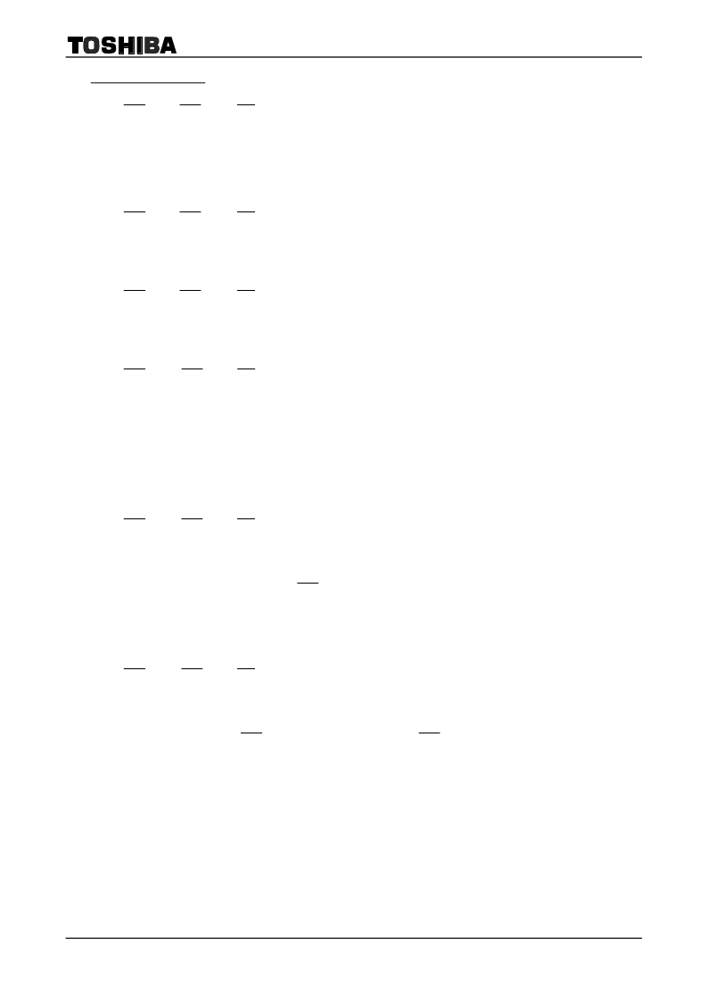
1. Command Function
1-1
Bank Activate command
(RAS
=
L, CAS
=
H, WE
=
H, BS0, BS1
=
Bank, A0~A12
=
Row Address)
The Bank Activate command activates the bank designated by the BS (Bank Select) signal.
Row addresses are latched on A0~A12 when this command is issued and the cell data is read out to the
sense amplifiers. The maximum time that each bank can be held in the active state is specified as t
RAS
(max).
1-2
Bank Precharge command
(RAS
=
L, CAS
=
H, WE
=
L, BS0, BS1
=
Bank, A10
=
L, A0~A9, A11, A12
=
Don’t care)
The Bank Precharge command precharges the bank designated by BS. The precharged bank is
switched from the active state to the idle state.
1-3
Precharge All command
(RAS
=
L, CAS
=
H, WE
=
L, BS0, BS1
=
Don’t care, A10
=
H, A0~A9, A11, A12
=
Don’t care)
The Precharge All command precharges all banks simultaneously. All banks are then switched to the
idle state.
1-4
Write command
(RAS
=
H, CAS
=
L, WE
=
L, BS0, BS1
=
Bank, A10
=
L, A0~A9, A11
=
Column Address, A12
=
Don’t
care)
The Write command performs a Write operation to the bank designated by BS0 and BS1. The write
data is latched at the positive edges of CLK. The length of the write data (Burst Length) and column
access sequence (Addressing Mode) must be programmed in the Mode Resister at power-up prior to the
Write operation.
The A11 input is “Don’t care” on the TC59SM808BFT/BFTL and the A9 and A11 inputs are “Don’t care”
on the TC59SM816BFT/BFTL.
1-5
Write with Auto Precharge command
(RAS
=
H, CAS
=
L, WE
=
L, BS0, BS1
=
Bank, A10
=
H, A0~A9, A11
=
Column Address, A12
=
Don’t
care)
The Write with Auto Precharge command performs the Precharge operation automatically after the
Write operation. The internal precharge starts in the cycles immediately following the cycle in which the
last data is written independent of CAS Latency (Figure 16). This command must not be interrupted by
any other commands.
The A11 input is “Don’t care” at the TC59SM808BFT/BFTL and the A9 and A11 inputs are “Don’t care”
on the TC59SM816BFT/BFTL.
1-6
Read command
(RAS
=
H, CAS
=
L, WE
=
H, BS0, BS1
=
Bank, A10
=
L, A0~A9, A11
=
Column Address, A12
=
Don’t
care)
The Read command performs a Read operation to the bank designated by BS. The read data is issued
sequentially synchronized to the positive edges of CLK. The length of read data (Burst Length),
Addressing Mode and CAS Latency (access time from CAS command in a clock cycle) must be
programmed in the Mode Register at power-up prior to the Write operation.
The A11 input is “Don’t care” on the TC59SM808BFT/BFTL and the A9 and A11 inputs are “Don’t care”
on the TC59SM816BFT/BFTL.
相關(guān)PDF資料 |
PDF描述 |
|---|---|
| TCS59SM816BFTL-80 | 4M×4Banks×16Bits Synchronous DRAM(4組4M×16位同步動(dòng)態(tài)RAM) |
| TCS800 | 800 Watts, 50 Volts, Pulsed Avionics 1030 MHz |
| TD-76 | MICROWAVE NOISE TUBES & NOISE SOURCES |
| TD-10 | MICROWAVE NOISE TUBES & NOISE SOURCES |
| TD-11 | MICROWAVE NOISE TUBES & NOISE SOURCES |
相關(guān)代理商/技術(shù)參數(shù) |
參數(shù)描述 |
|---|---|
| TCS5BB6A0 | 制造商:Digital Persona 功能描述:SPI USB - TRAY STAINLESS STEEL BEZEL - Trays 制造商:UPEK 功能描述:SPI USB - TRAY STAINLESS STEEL BEZEL - Trays |
| TCS5BB6A2 | 制造商:Digital Persona 功能描述:TCS5B (USB CHIPSET) REEL STAINLESS STEEL BEZEL SMALL PACKAGE - Bulk 制造商:UPEK 功能描述:TCS5B (USB CHIPSET) REEL STAINLESS STEEL BEZEL SMALL PACKAGE - Bulk |
| TCS5BE6B1 | 制造商:Digital Persona 功能描述:TCS5BE6B1 - Bulk 制造商:UPEK 功能描述:TCS5BE6B1 - Bulk |
| TCS5BF6A1 | 制造商:Digital Persona 功能描述:TCS5B (USB CHIPSET) TRAY STAINLESS STEEL BEZEL LARGE PACKAGE - Bulk 制造商:UPEK 功能描述:TCS5B (USB CHIPSET) TRAY STAINLESS STEEL BEZEL LARGE PACKAGE - Bulk |
| TCS5BF6A2 | 制造商:Digital Persona 功能描述:TCS5B (USB CHIPSET) REEL STAINLESS STEEL BEZEL LARGE PACKAGE - Bulk 制造商:UPEK 功能描述:TCS5B (USB CHIPSET) REEL STAINLESS STEEL BEZEL LARGE PACKAGE - Bulk |
發(fā)布緊急采購,3分鐘左右您將得到回復(fù)。