- 您現(xiàn)在的位置:買(mǎi)賣(mài)IC網(wǎng) > PDF目錄372239 > SRM20V512SLTT7 x8 SRAM PDF資料下載
參數(shù)資料
| 型號(hào): | SRM20V512SLTT7 |
| 英文描述: | x8 SRAM |
| 中文描述: | x8的SRAM |
| 文件頁(yè)數(shù): | 4/8頁(yè) |
| 文件大小: | 85K |
| 代理商: | SRM20V512SLTT7 |
SRM20V512SLMT
7
4
Note)
6
1 During read cycle time, WE is to be "H" level.
6
2 During write cycle time that is controlled by CS1 or CS2, Input/output Buffer is in high impedance state whether OE level is "H"or
"L".
6
3 During write cycle time that is controlled by WE, Input/output Buffer is high impedance state if OE is "H" level.
6
4 When I/O terminals are output mode, be careful that do not give the epposite signals to the I/O terminals.
G
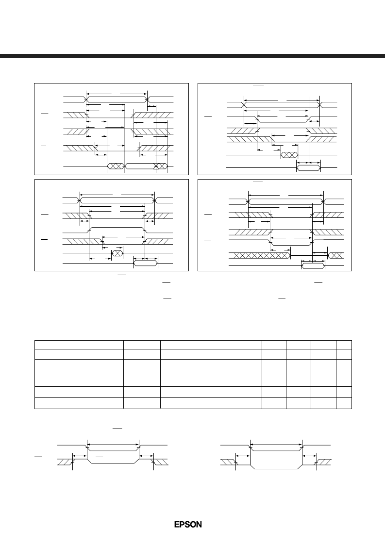
Timing Chart
H
Read Cycle
6
1
H
Write Cycle 1 (CS1 Control)
6
2
H
Write Cycle 3 (WE Control)
6
3
6
4
H
Write Cycle 2 (CS2 Control)
6
2
Address
CS1
CS2
WE
Dout
Din
t
WC
t
AW
t
WP
t
DW
t
WR
t
AS
t
WHZ
t
OW
t
Address
CS1
CS2
WE
Dout
Din
t
WC
t
AW
t
CW2
t
WP
t
CLZ2
t
WHZ
t
DW
t
WR
t
AS
t
DH
Address
CS1
CS2
OE
Dout
Address
CS1
CS2
WE
Dout
Din
t
WC
t
AW
t
WP
t
CW1
t
WHZ
t
CLZ1
t
DW
t
WR
t
AS
t
DH
t
OH
t
CHZ1
ACS2
t
CLZ2
t
CHZ2
t
OE
t
OHZ
t
OLZ
t
RC
t
ACC
t
ACS1
t
CLZ1
G
DATA RETENTION CHARACTERISTIC WITH LOW VOLTAGE POWER SUPPLY
Parameter
Symbol
Conditions
Min.
Typ.
6
—
Max.
Unit
Data retention supply voltage
Data retention current
Chip select data hold time
V
DDR
I
DDR
t
CDR
2.0
3.6
25
V
ns
(V
SS
= 0V, Ta = –40 to 85
°
C)
0
5
Operation recovery time
t
R
ms
V
DD
= 2.7V
CS1 = CS2
≥
V
DD
–0.2V
or CS2
≤
0.2V
6
: Ta = 25
°
C
0.25
—
μ
A
—
—
—
—
Data retention timing 1 (CS1 Control)
V
DD
CS1
V
DDR
≥
2.0V
CS1
≥
V
DD
\
0.2V
Data hold mode
t
CDR
V
IH
2.7V
2.7V
t
R
2.7V
t
CDR
2.7V
t
R
V
IH
Date retention timing 2 (CS2 Control)
V
DD
CS2
V
DDR
≥
2.0V
CS2
≤
0.2V
Data hold mode
V
IL
V
IL
相關(guān)PDF資料 |
PDF描述 |
|---|---|
| SRM2114C25 | x4 SRAM |
| SRM2114CL7 | x4 SRAM |
| SRM2114M25 | x4 SRAM |
| SRM2114ML7 | x4 SRAM |
| SRM2AL256LLM | x8 SRAM |
相關(guān)代理商/技術(shù)參數(shù) |
參數(shù)描述 |
|---|---|
| SRM20V512SLTX7 | 制造商:未知廠(chǎng)家 制造商全稱(chēng):未知廠(chǎng)家 功能描述:x8 SRAM |
| SRM20V512SLYX7 | 制造商:未知廠(chǎng)家 制造商全稱(chēng):未知廠(chǎng)家 功能描述:x8 SRAM |
| SRM2114C25 | 制造商:未知廠(chǎng)家 制造商全稱(chēng):未知廠(chǎng)家 功能描述:x4 SRAM |
| SRM2114CL7 | 制造商:未知廠(chǎng)家 制造商全稱(chēng):未知廠(chǎng)家 功能描述:x4 SRAM |
| SRM2114M25 | 制造商:未知廠(chǎng)家 制造商全稱(chēng):未知廠(chǎng)家 功能描述:x4 SRAM |
發(fā)布緊急采購(gòu),3分鐘左右您將得到回復(fù)。