- 您現(xiàn)在的位置:買賣IC網(wǎng) > PDF目錄373427 > SMJ320MCM41A (Texas Instruments, Inc.) Single SMJ320C40 Mutichip Module(單SMJ320C40多芯片組件) PDF資料下載
參數(shù)資料
| 型號: | SMJ320MCM41A |
| 廠商: | Texas Instruments, Inc. |
| 英文描述: | Single SMJ320C40 Mutichip Module(單SMJ320C40多芯片組件) |
| 中文描述: | 單SMJ320C40 Mutichip模塊(單SMJ320C40多芯片組件) |
| 文件頁數(shù): | 7/12頁 |
| 文件大小: | 259K |
| 代理商: | SMJ320MCM41A |

SMJ320MCM41A
SINGLE SMJ320C40 MULTICHIP MODULE
SGMS719 – JUNE 1995
7
POST OFFICE BOX 1443
HOUSTON, TEXAS 77251–1443
reference documentation and data sheet scope
The SMJ320MCM41A is qualified to MIL-I-38535. Electrical continuity of the module is assured through use of
IEEE-1149.1-compatible boundary-scan testing and functional checkout of local SRAM space.
KGD refers to Texas Instruments known-good-die strategy. TI KGDs are fully tested over the military
temperature range and burned in per MIL-STD-883. Electrical test assures compliance of the ’C40 KGD
components to the SMJ320C40 data sheet (SGUS017) over the operating temperature range. Module timings
are virtually unchanged from the SMJ320C40 data sheet timings. An SMJ320C40 data sheet is provided for
customer reference only and does not imply MCM compliance to published timings.
For a complete description of the ’C40 operation and application information, refer to the TMS320C4x User’s
Guide(SPRU063A).
absolute maximum ratings over operating free-air temperature (unless otherwise noted)
Supply voltage range, V
CC
(see Note 1)
. . . . . . . . . . . . . . . . . . . . . . . . . . . . . . . . . . . . . . . . . . . . .
Voltage range on any pin
. . . . . . . . . . . . . . . . . . . . . . . . . . . . . . . . . . . . . . . . . . . . . . . . . . . . . . . . . .
Output voltage range, V
O
. . . . . . . . . . . . . . . . . . . . . . . . . . . . . . . . . . . . . . . . . . . . . . . . . . . . . . . . . .
Storage temperature range, T
stg
. . . . . . . . . . . . . . . . . . . . . . . . . . . . . . . . . . . . . . . . . . . . . . . . . .
Stresses beyond those listed under “absolute maximum ratings” may cause permanent damage to the device. These are stress ratings only, and
functional operation of the device at these or any other conditions beyond those indicated under “recommended operating conditions” is not
implied. Exposure to absolute-maximum-rated conditions for extended periods may affect device reliability.
NOTE 1: All voltage values are with respect to VSS.
– 0.3 V to 7 V
– 0.3 V to 7 V
– 0.3 V to 7 V
– 65
°
C to 150
°
C
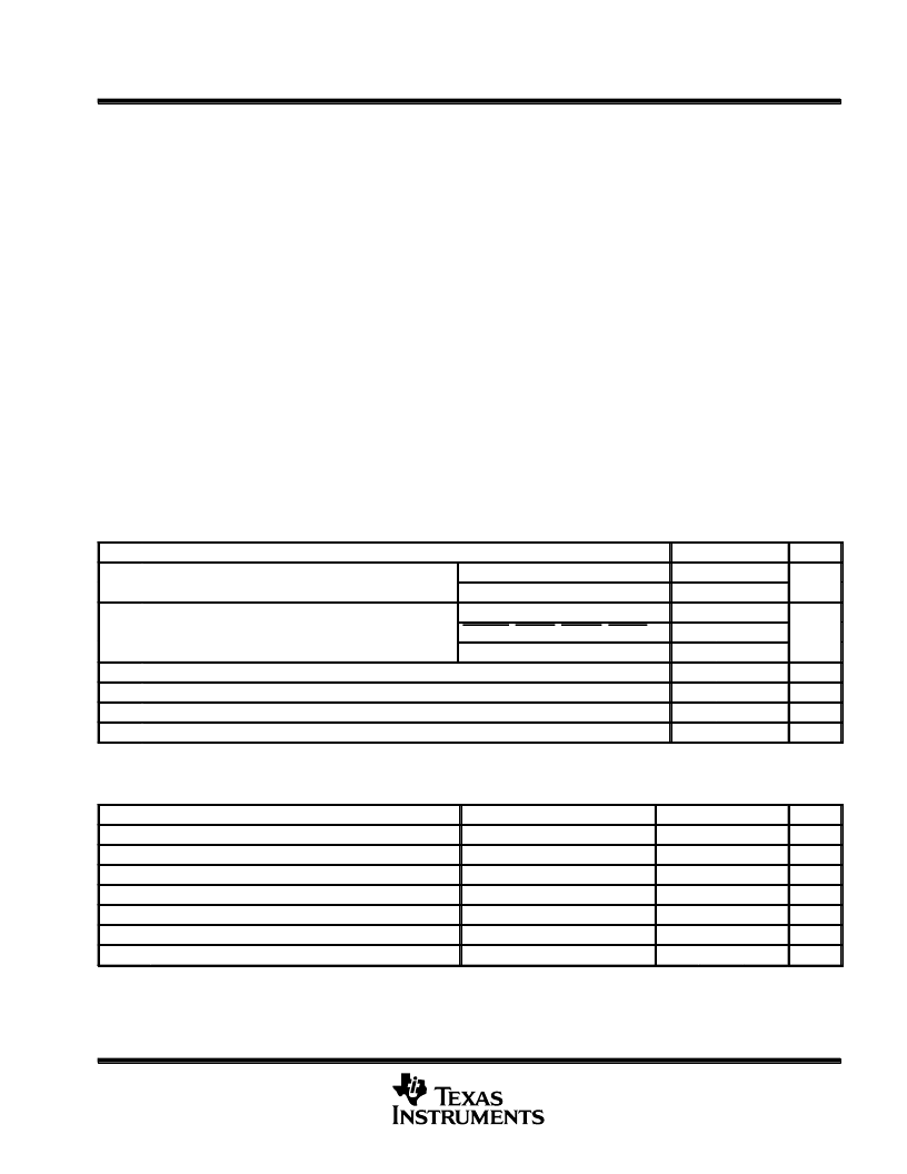
recommended operating conditions
MIN
4.5
MAX
5.5
UNIT
VCC
Supply voltage
’MCM41A-33
V
’MCM41A-40
4.75
5.25
VIH
Hi h l
High-level input voltage
CLKIN
2.6
VCC+ 0.3
VCC+ 0.3
VCC+ 0.3
0.8
V
CSTRBx, CRDYx, CREQx, CACKx
2.2
All others
2
VIL
IOH
IOL
TJ
Low-level input voltage
– 0.3
V
μ
A
mA
°
C
High-level output current
– 300
Low-level output current
2
Operating junction temperature
– 55
125
electrical characteristics over recommended ranges of supply voltage and operating free-air
temperature
PARAMETER
TEST CONDITIONS
MIN
TYP
MAX
UNIT
VOH
VOL
ICC
IZ
II
IIP
IIC
For conditions shown as MIN/MAX, use the appropriate value specified under recommended operating conditions.
NOTE 2: Pins with internal pullup devices TDI, TCK, TMS
High-level output voltage
VCC = MIN,
VCC = MAX
VI = VSS to VCC
VI = VSS to VCC
VI = VSS to VCC
VI = VSS to VCC
IOH = MAX
IOL = MAX
2.4
3
V
Low-level output voltage
0.3
0.6
V
Supply current
0.4
0.6
A
μ
A
μ
A
μ
A
μ
A
Three-state current
– 20
20
Input current
– 10
10
Input current, internal pullup (see Note 2)
– 400
30
Input current, CLKIN
– 50
50
A
相關(guān)PDF資料 |
PDF描述 |
|---|---|
| SMJ34020AGB | GRAPHICS SYSTEM PROCESSOR |
| SMJ34020AHT | GRAPHICS SYSTEM PROCESSOR |
| SMJ4256 | 262,144-BIT DYNAMIC RANDOM-ACCESS MEMORY |
| SMJ4256FV | 262,144-BIT DYNAMIC RANDOM-ACCESS MEMORY |
| SMJ4256JD | 262,144-BIT DYNAMIC RANDOM-ACCESS MEMORY |
相關(guān)代理商/技術(shù)參數(shù) |
參數(shù)描述 |
|---|---|
| SMJ320MCM41DHFHM40 | 制造商:Rochester Electronics LLC 功能描述:- Bulk |
| SMJ320MCM42C | 制造商:TI 制造商全稱:Texas Instruments 功能描述:DUAL SMJ320C40 MULTICHIP MODULE |
| SMJ320MCM42CHFN | 制造商:TI 制造商全稱:Texas Instruments 功能描述:DUAL SMJ320C40 MULTICHIP MODULE |
| SMJ320MCM42D | 制造商:TI 制造商全稱:Texas Instruments 功能描述:DUAL SMJ320C40 MULTICHIP MODULE |
| SMJ320MCM42DHFN | 制造商:TI 制造商全稱:Texas Instruments 功能描述:DUAL SMJ320C40 MULTICHIP MODULE |
發(fā)布緊急采購,3分鐘左右您將得到回復(fù)。