- 您現(xiàn)在的位置:買賣IC網(wǎng) > PDF目錄373427 > SMJ320MCM41A (Texas Instruments, Inc.) Single SMJ320C40 Mutichip Module(單SMJ320C40多芯片組件) PDF資料下載
參數(shù)資料
| 型號(hào): | SMJ320MCM41A |
| 廠商: | Texas Instruments, Inc. |
| 英文描述: | Single SMJ320C40 Mutichip Module(單SMJ320C40多芯片組件) |
| 中文描述: | 單SMJ320C40 Mutichip模塊(單SMJ320C40多芯片組件) |
| 文件頁(yè)數(shù): | 10/12頁(yè) |
| 文件大?。?/td> | 259K |
| 代理商: | SMJ320MCM41A |
SMJ320MCM41A
SINGLE SMJ320C40 MULTICHIP MODULE
SGMS719 – JUNE 1995
10
POST OFFICE BOX 1443
HOUSTON, TEXAS 77251–1443
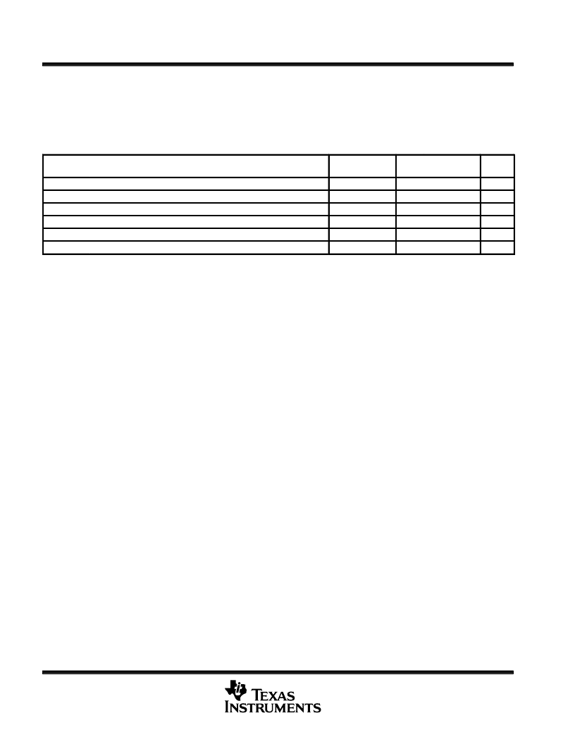
thermal analysis
Thermal conduction of components in the SMJ320MCM41A is dependent on thermal resistance of the material
under each die as well as die area thermally connected to the heat dissipating medium. Since these properties
vary with layout and die size, ’C40 and SRAM components should be considered separately. The following table
lists primary parameters required for thermal analysis of the module. The junction temperature, T
J
, is not to be
exceeded for ’C40s or SRAM die.
PARAMETER
ALTERNATE
SYMBOL
MIN
TYP
MAX
UNIT
TJ
PT1
PT4
Z0JC1
Z0JC2
Junction temperature under operating condition
TJ
PC40
PSRAM
TJC-C40
TJC-SRAM
TSOL
125
°
C
W
Individual ’C40 power dissipation (1 per module)
1.75
4.4
Individual SRAM power dissipation (4 per module)
0.25
0.8
W
Thermal impedance (junction to case) for ’C40 die
2.3
°
C/W
°
C/W
°
C
Thermal impedance (junction to case) for SRAM die
4.3
Maximum solder temperature (10 s duration)
260
power estimation
The power requirements of the ’320MCM41A have been characterized over the operating temperature range.
See the application report Calculation of TMS320C40 Power Dissipation(SPRA032) as reference for power
estimation of the ’C40 components.
Typical power dissipation has been measured with the ’C40s executing a 64-point FFT algorithm. Input and
output data arrays resided in module SRAM, and output data was written out to the global-address space. The
global databus was loaded with 80-pF test loads, and both local and global writes were configured for
0-wait-state memory. Under typical conditions of 25
°
C, 5-V V
CC
, and 40-MHz CLKIN frequency, the power
dissipation was measured to be 1.75 W.
Maximum power dissipation has been measured under worst case conditions. The global databus was loaded
with 80-pF test loads, and simultaneous 0-wait-state writes have been performed to both local and global buses.
Under worst case environment conditions of – 55
°
C, 5.25-V V
CC
, and 40-MHz CLKIN frequency, the power
dissipation was determined to be 3 W. The algorithm executed during these tests consists of parallel writes of
alternating 0xAAs and 0x55s to both local SRAM and global-address spaces. This algorithm is not considered
to be a practical use of the ’C40’s resources; therefore, the associated power measurement should be
considered absolute maximum only.
A
相關(guān)PDF資料 |
PDF描述 |
|---|---|
| SMJ34020AGB | GRAPHICS SYSTEM PROCESSOR |
| SMJ34020AHT | GRAPHICS SYSTEM PROCESSOR |
| SMJ4256 | 262,144-BIT DYNAMIC RANDOM-ACCESS MEMORY |
| SMJ4256FV | 262,144-BIT DYNAMIC RANDOM-ACCESS MEMORY |
| SMJ4256JD | 262,144-BIT DYNAMIC RANDOM-ACCESS MEMORY |
相關(guān)代理商/技術(shù)參數(shù) |
參數(shù)描述 |
|---|---|
| SMJ320MCM41DHFHM40 | 制造商:Rochester Electronics LLC 功能描述:- Bulk |
| SMJ320MCM42C | 制造商:TI 制造商全稱:Texas Instruments 功能描述:DUAL SMJ320C40 MULTICHIP MODULE |
| SMJ320MCM42CHFN | 制造商:TI 制造商全稱:Texas Instruments 功能描述:DUAL SMJ320C40 MULTICHIP MODULE |
| SMJ320MCM42D | 制造商:TI 制造商全稱:Texas Instruments 功能描述:DUAL SMJ320C40 MULTICHIP MODULE |
| SMJ320MCM42DHFN | 制造商:TI 制造商全稱:Texas Instruments 功能描述:DUAL SMJ320C40 MULTICHIP MODULE |
發(fā)布緊急采購(gòu),3分鐘左右您將得到回復(fù)。