- 您現(xiàn)在的位置:買賣IC網(wǎng) > PDF目錄98084 > SMJ320C6414DGADW60 (TEXAS INSTRUMENTS INC) 64-BIT, 75 MHz, OTHER DSP, CPGA570 PDF資料下載
參數(shù)資料
| 型號: | SMJ320C6414DGADW60 |
| 廠商: | TEXAS INSTRUMENTS INC |
| 元件分類: | 數(shù)字信號處理 |
| 英文描述: | 64-BIT, 75 MHz, OTHER DSP, CPGA570 |
| 封裝: | 33 X 33 MM, CERAMIC, FCPGA-570 |
| 文件頁數(shù): | 21/134頁 |
| 文件大?。?/td> | 1997K |
| 代理商: | SMJ320C6414DGADW60 |
第1頁第2頁第3頁第4頁第5頁第6頁第7頁第8頁第9頁第10頁第11頁第12頁第13頁第14頁第15頁第16頁第17頁第18頁第19頁第20頁當前第21頁第22頁第23頁第24頁第25頁第26頁第27頁第28頁第29頁第30頁第31頁第32頁第33頁第34頁第35頁第36頁第37頁第38頁第39頁第40頁第41頁第42頁第43頁第44頁第45頁第46頁第47頁第48頁第49頁第50頁第51頁第52頁第53頁第54頁第55頁第56頁第57頁第58頁第59頁第60頁第61頁第62頁第63頁第64頁第65頁第66頁第67頁第68頁第69頁第70頁第71頁第72頁第73頁第74頁第75頁第76頁第77頁第78頁第79頁第80頁第81頁第82頁第83頁第84頁第85頁第86頁第87頁第88頁第89頁第90頁第91頁第92頁第93頁第94頁第95頁第96頁第97頁第98頁第99頁第100頁第101頁第102頁第103頁第104頁第105頁第106頁第107頁第108頁第109頁第110頁第111頁第112頁第113頁第114頁第115頁第116頁第117頁第118頁第119頁第120頁第121頁第122頁第123頁第124頁第125頁第126頁第127頁第128頁第129頁第130頁第131頁第132頁第133頁第134頁
SMJ320C6414, SMJ320C6415, SMJ320C6416
FIXEDPOINT DIGITAL SIGNAL PROCESSORS
SGUS050A JANUARY 2004 REVISED MARCH 2004
117
POST OFFICE BOX 1443
HOUSTON, TEXAS 772511443
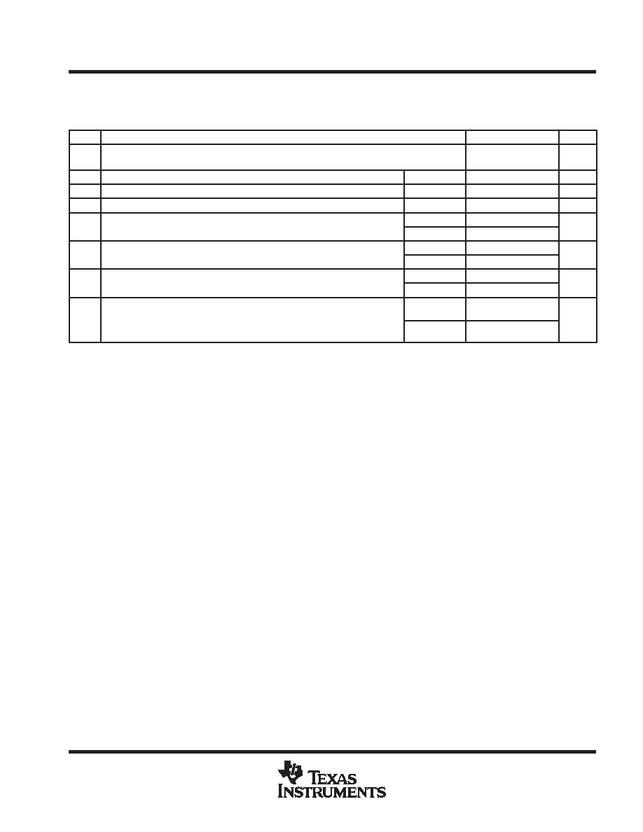
MULTICHANNEL BUFFERED SERIAL PORT (McBSP) TIMING (CONTINUED)
switching characteristics over recommended operating conditions for McBSP (see Figure 51)
NO.
PARAMETER
MIN
MAX
UNIT
1
td(CKSH-CKRXH)
Delay time, CLKS high to CLKR/X high for internal CLKR/X generated
from CLKS input
1.4
10
ns
2
tc(CKRX)
Cycle time, CLKR/X
CLKR/X int
6.67§*
ns
3
tw(CKRX)
Pulse duration, CLKR/X high or CLKR/X low
CLKR/X int
C 1*
C + 1*
ns
4
td(CKRH-FRV)
Delay time, CLKR high to internal FSR valid
CLKR int
2.1
3
ns
9
td(CKXH-FXV)
Delay time, CLKX high to internal FSX valid
CLKX int
1.7
3
ns
9
td(CKXH-FXV)
Delay time, CLKX high to internal FSX valid
CLKX ext
1.7
9
ns
12
tdis(CKXH-DXHZ)
Disable time, DX high impedance following last data bit
CLKX int
3.9*
4*
ns
12
tdis(CKXH-DXHZ)
Disable time, DX high impedance following last data bit
from CLKX high
CLKX ext
2.1*
9*
ns
13
td(CKXH-DXV)
Delay time, CLKX high to DX valid
CLKX int
3.9 + D1#
4 + D2#
ns
13
td(CKXH-DXV)
Delay time, CLKX high to DX valid
CLKX ext
2.1 + D1#
9 + D2#
ns
14
td(FXH-DXV)
Delay time, FSX high to DX valid
FSX int
2.3
5.6
ns
14
td(FXH-DXV)
ONLY applies when in data
delay 0 (XDATDLY = 00b) mode
FSX ext
1.9
9
ns
*This parameter is not production tested.
CLKRP = CLKXP = FSRP = FSXP = 0. If polarity of any of the signals is inverted, then the timing references of that signal are also inverted.
Minimum delay times also represent minimum output hold times.
§ Minimum CLKR/X cycle times are based on internal logic speed; the maximum usable speed may be lower due to EDMA limitations and AC timing
requirements.
C = H or L
S =
sample rate generator input clock = 4P if CLKSM = 1 (P = 1/CPU clock frequency)
=
sample rate generator input clock = P_clks if CLKSM = 0 (P_clks = CLKS period)
H =
CLKX high pulse width = (CLKGDV/2 + 1) * S if CLKGDV is even
= (CLKGDV + 1)/2 * S if CLKGDV is odd or zero
L =
CLKX low pulse width
= (CLKGDV/2) * S if CLKGDV is even
= (CLKGDV + 1)/2 * S if CLKGDV is odd or zero
CLKGDV should be set appropriately to ensure the McBSP bit rate does not exceed the maximum limit (see footnote above).
# Extra delay from CLKX high to DX valid applies only to the first data bit of a device, if and only if DXENA = 1 in SPCR.
if DXENA = 0, then D1 = D2 = 0
if DXENA = 1, then D1 = 4P, D2 = 8P
相關(guān)PDF資料 |
PDF描述 |
|---|---|
| SM320C6414DGADW60 | 64-BIT, 75 MHz, OTHER DSP, CPGA570 |
| SM320C6416DGADW60 | 64-BIT, 75 MHz, OTHER DSP, CPGA570 |
| SMJ320C6701GLPW16 | 32-BIT, 166.66 MHz, OTHER DSP, CBGA429 |
| SMJ34010-50FDM | GRAPHICS PROCESSOR, CQCC68 |
| SMJ34010-40GBM | GRAPHICS PROCESSOR, CPGA68 |
相關(guān)代理商/技術(shù)參數(shù) |
參數(shù)描述 |
|---|---|
| SMJ320C6415 | 制造商:TI 制造商全稱:Texas Instruments 功能描述:FIXED-POINT DIGITAL SIGNAL PROCESSORS |
| SMJ320C6415C | 制造商:TI 制造商全稱:Texas Instruments 功能描述:FIXED-POINT DIGITAL SIGNAL PROCESSORS |
| SMJ320C6415D | 制造商:TI 制造商全稱:Texas Instruments 功能描述:FIXED-POINT DIGITAL SIGNAL PROCESSORS |
| SMJ320C6415DGADW60 | 制造商:Texas Instruments 功能描述: 制造商:Texas Instruments 功能描述:TISSMJ320C6415DGADW60 MIL SPEC FIXED DSP |
| SMJ320C6416 | 制造商:TI 制造商全稱:Texas Instruments 功能描述:FIXED-POINT DIGITAL SIGNAL PROCESSORS |
發(fā)布緊急采購,3分鐘左右您將得到回復。