- 您現(xiàn)在的位置:買賣IC網(wǎng) > PDF目錄378699 > SM8213 (Seiko NPC Corporation) MINIATURE POWER RELAY PDF資料下載
參數(shù)資料
| 型號: | SM8213 |
| 廠商: | Seiko NPC Corporation |
| 英文描述: | MINIATURE POWER RELAY |
| 中文描述: | POCSAG碼解碼器多幀尋呼機 |
| 文件頁數(shù): | 16/33頁 |
| 文件大?。?/td> | 171K |
| 代理商: | SM8213 |
第1頁第2頁第3頁第4頁第5頁第6頁第7頁第8頁第9頁第10頁第11頁第12頁第13頁第14頁第15頁當前第16頁第17頁第18頁第19頁第20頁第21頁第22頁第23頁第24頁第25頁第26頁第27頁第28頁第29頁第30頁第31頁第32頁第33頁
SM8213AM
NIPPON PRECISION CIRCUITS—16
Received Data Transmission (SM8213AM to CPU)
In lock mode, if the receive data for the frame is rec-
ognized as one of the 28 normal addresses or a
dummy address with 2 bit errors or less, then the data
is temporarily stored in the transmit buffer and then
error correction and other processing takes place.
After processing, ATTN goes LOW to inform the
CPU that transmit ready data is available.
The SM8213AM switches the data internally and
then outputs 32-bit data, shown in table 7, on SDO in
sync with the falling edge of the SCK clock. The
CPU can then read the data on either the SCK rising
edge or the falling edge.
The message bits (1 to 20), which are the 13th to
32nd bits of the detected address data, comprises 18
address information bits and 2 function bits.
When the 32-bit transmission ends, ATTN goes
HIGH to indicate that all necessary information has
been transmitted.
When an address is detected, the next 32-bit data
code word is received. The BCH(31,21) format error
check bits are checked and if a 1-bit or two consecu-
tive bit errors occur, they are corrected. Two random
bit errors, or three or more bit errors are not cor-
rected.
If the corrected data MSB is 1, the data is recognized
as a message, data reception continues and the cor-
rected message data and error check flags are sent to
the CPU as 32-bit data, shown in table 7, with the
same data handling as an address. In this case also,
ATTN goes LOW after processing to inform the
CPU that transmit ready data is available. The time
from when ATTN goes LOW until the CPU sends the
SCK should be the same as shown in figure 9. Also,
when the message continues, the normal SCK clock
speed becomes faster than the receive signal bit rate
and as a result there is a limit to the transmitted
information capacity. As ATTN is used as the trans-
mit ready data available signal output, it can be used
as the CPU interrupt signal to receive data with the
timing shown in figure 9.
Conversely, when the decoder takes ATTN LOW to
indicate transmit ready data is available, the micro-
controller operates under normal starting conditions
(high-speed clock operation), and 32-bit clock is
input on SCK. After data is read in and until ATTN
goes LOW for the next transmit ready data signal,
the series processing should be such that it takes less
than {32
×
(bit rate)} time. If it takes longer than this
amount of time, the succeeding data may not be out-
put correctly.
When the MSB is 0 and data is recognized as an idle
signal or idle code, data reception and data transfer
to the CPU stops after the end-of-message is output
for addresses not matching the self address.
However, when CPU BREAK input interrupt end-of-
message method is selected (see “Flag Setting” sec-
tion), data is treated as a message and reception con-
tinues even if the MSB is 0.
When sending data from the decoder to the micro-
controller, the SCK clock frequency should not be
less than 512, (1200), [2400] Hz. If this occurs, the
SCK counter is reinitialized. This function, however,
does make restoring operation easy even if this or
another clock is accidentally input.
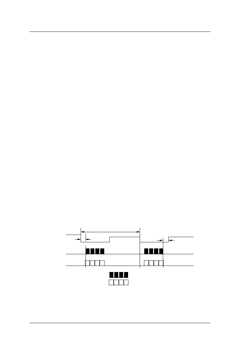
Figure 9. Received data transmit timing
ATTN
SCK
SDO
D A T A
D A T A
D A T A
:
8-bit
×
4-byte = 32-bit unit time clock
:
8-bit
×
4-byte = 32-bit unit time data
Refer to the AC Characteristics section for detailed timing specifications.
0ms min
32 bit time
0ms min
相關(guān)PDF資料 |
PDF描述 |
|---|---|
| SM8213AM | POCSAG Decoder For Multiframe Pagers |
| SM8220 | Calling Number Identification Receiver IC |
| SM8221 | Calling Number Identification Receiver IC |
| SM8222 | Caller ID Service IC with Call Waiting |
| SM8222A | Caller ID Service IC with Call Waiting |
相關(guān)代理商/技術(shù)參數(shù) |
參數(shù)描述 |
|---|---|
| SM8213AM | 制造商:NPC 制造商全稱:Nippon Precision Circuits Inc 功能描述:POCSAG Decoder For Multiframe Pagers |
| SM821C906ZAA | 制造商:AVX Corporation 功能描述:- Bulk |
| SM8220 | 制造商:NPC 制造商全稱:Nippon Precision Circuits Inc 功能描述:Calling Number Identification Receiver IC |
| SM8221 | 制造商:NPC 制造商全稱:Nippon Precision Circuits Inc 功能描述:Calling Number Identification Receiver IC |
| SM8222 | 制造商:NPC 制造商全稱:Nippon Precision Circuits Inc 功能描述:Caller ID Service IC with Call Waiting |
發(fā)布緊急采購,3分鐘左右您將得到回復(fù)。