- 您現(xiàn)在的位置:買賣IC網(wǎng) > PDF目錄378699 > SM8213 (Seiko NPC Corporation) MINIATURE POWER RELAY PDF資料下載
參數(shù)資料
| 型號(hào): | SM8213 |
| 廠商: | Seiko NPC Corporation |
| 英文描述: | MINIATURE POWER RELAY |
| 中文描述: | POCSAG碼解碼器多幀尋呼機(jī) |
| 文件頁數(shù): | 1/33頁 |
| 文件大?。?/td> | 171K |
| 代理商: | SM8213 |
當(dāng)前第1頁第2頁第3頁第4頁第5頁第6頁第7頁第8頁第9頁第10頁第11頁第12頁第13頁第14頁第15頁第16頁第17頁第18頁第19頁第20頁第21頁第22頁第23頁第24頁第25頁第26頁第27頁第28頁第29頁第30頁第31頁第32頁第33頁
SM8213AM
NIPPON PRECISION CIRCUITS—1
NIPPON PRECISION CIRCUITS INC.
POCSAG Decoder For Multiframe Pagers
OVERVIEW
The SM8213AM is a POCSAG-standard (Post
Office Code Standardization Advisory Group) signal
processor LSI, which conforms to CCIR recommen-
dation 584 concerning standard international wire-
less calling codes.
The SM8213AM supports call messages in either
tone, numerical or character outputs at signal speeds
of 512, 1200 or 2400 bps. The signal input stage fea-
tures a built-in filter.
Each of the addresses (max. 7 + 1 dummy = 8) can
be assigned to any frame, which also makes the
device configurable for many additional services.
Each address can be independently set to ON/OFF.
Furthermore, built-in buffer memory means decoded
information can be fetched in sync with the micro-
controller clock, thereby reducing the microcontrol-
ler CPU time required. Intermittent-duty method
(battery saving (BS) method) control signals, com-
patible with PLL operation, and Molybdenum-gate
CMOS structure makes possible the construction of
low-voltage operation, low power dissipation sys-
tems.
The SM8213AM is available in 16-pin SSOPs.
FEATURES
I
Conforms to POCSAG standard for pagers
512, 1200 or 2400 bps signal speed
Multiframe compatible (each address individually
controllable)
8 addresses
×
4 sub-addresses (total of 32
addresses) control
(8 addresses comprise 7 actual addresses + 1
dummy address)
Built-in buffer memory (1 code word)
Supports tone, numeric or character call messages
Built-in input signal filter, with filter ON/OFF and
4 selectable filter characteristics
PLL-compatible battery saving method (BS1,
BS2, BS3 outputs)
BS1 (RF control main output signal) 61-step setup
time setting
BS3 (PLL setup signal) 61-step setup time setting
BS2 (RF DC-level adjustment signal) before/dur-
ing reception selectable adjustment timing
1-bit and 2-bit burst error auto-correction function
I
I
I
I
I
I
I
I
I
I
I
I
25 to 75% duty factor signal coverage
8 rate error detection condition settings
76.8 kHz system clock (crystal oscillator)
76.8 or 38.4 kHz clock output pin
Built-in oscillator capacitor and feedback resistor
2.0 to 3.5 V operating supply voltage
Molybdenum-gate CMOS process realizes low
power dissipation
16-pin SSOP
I
I
I
I
I
I
I
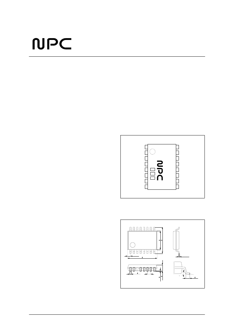
PINOUT
Top View
PACKAGE DIMENSIONS
Unit: mm
ATTN
SDI
SDO
SCK
AREA
RSTN
BS1
BS2
BS3
VDD
XVSS
XT
XTN
VSS
CLKO
SIGNAL
8
1
8
9
16
0.6TYP
6.8 0.3
0.8
0.36 0.1
0.4 0.2
0 10
0.15
- 0.05
0
1
4
6
相關(guān)PDF資料 |
PDF描述 |
|---|---|
| SM8213AM | POCSAG Decoder For Multiframe Pagers |
| SM8220 | Calling Number Identification Receiver IC |
| SM8221 | Calling Number Identification Receiver IC |
| SM8222 | Caller ID Service IC with Call Waiting |
| SM8222A | Caller ID Service IC with Call Waiting |
相關(guān)代理商/技術(shù)參數(shù) |
參數(shù)描述 |
|---|---|
| SM8213AM | 制造商:NPC 制造商全稱:Nippon Precision Circuits Inc 功能描述:POCSAG Decoder For Multiframe Pagers |
| SM821C906ZAA | 制造商:AVX Corporation 功能描述:- Bulk |
| SM8220 | 制造商:NPC 制造商全稱:Nippon Precision Circuits Inc 功能描述:Calling Number Identification Receiver IC |
| SM8221 | 制造商:NPC 制造商全稱:Nippon Precision Circuits Inc 功能描述:Calling Number Identification Receiver IC |
| SM8222 | 制造商:NPC 制造商全稱:Nippon Precision Circuits Inc 功能描述:Caller ID Service IC with Call Waiting |
發(fā)布緊急采購,3分鐘左右您將得到回復(fù)。