- 您現在的位置:買賣IC網 > PDF目錄373395 > Si3232-X-GQ (Electronic Theatre Controls, Inc.) DUAL PROGRAMMABLE CMOS SLIC WITH LINE MONITORING PDF資料下載
參數資料
| 型號: | Si3232-X-GQ |
| 廠商: | Electronic Theatre Controls, Inc. |
| 英文描述: | DUAL PROGRAMMABLE CMOS SLIC WITH LINE MONITORING |
| 中文描述: | 兩個可編程的CMOS用戶接口與在線監(jiān)測 |
| 文件頁數: | 37/128頁 |
| 文件大小: | 2327K |
| 代理商: | SI3232-X-GQ |
第1頁第2頁第3頁第4頁第5頁第6頁第7頁第8頁第9頁第10頁第11頁第12頁第13頁第14頁第15頁第16頁第17頁第18頁第19頁第20頁第21頁第22頁第23頁第24頁第25頁第26頁第27頁第28頁第29頁第30頁第31頁第32頁第33頁第34頁第35頁第36頁當前第37頁第38頁第39頁第40頁第41頁第42頁第43頁第44頁第45頁第46頁第47頁第48頁第49頁第50頁第51頁第52頁第53頁第54頁第55頁第56頁第57頁第58頁第59頁第60頁第61頁第62頁第63頁第64頁第65頁第66頁第67頁第68頁第69頁第70頁第71頁第72頁第73頁第74頁第75頁第76頁第77頁第78頁第79頁第80頁第81頁第82頁第83頁第84頁第85頁第86頁第87頁第88頁第89頁第90頁第91頁第92頁第93頁第94頁第95頁第96頁第97頁第98頁第99頁第100頁第101頁第102頁第103頁第104頁第105頁第106頁第107頁第108頁第109頁第110頁第111頁第112頁第113頁第114頁第115頁第116頁第117頁第118頁第119頁第120頁第121頁第122頁第123頁第124頁第125頁第126頁第127頁第128頁
Si3232
Preliminary Rev. 0.96
37
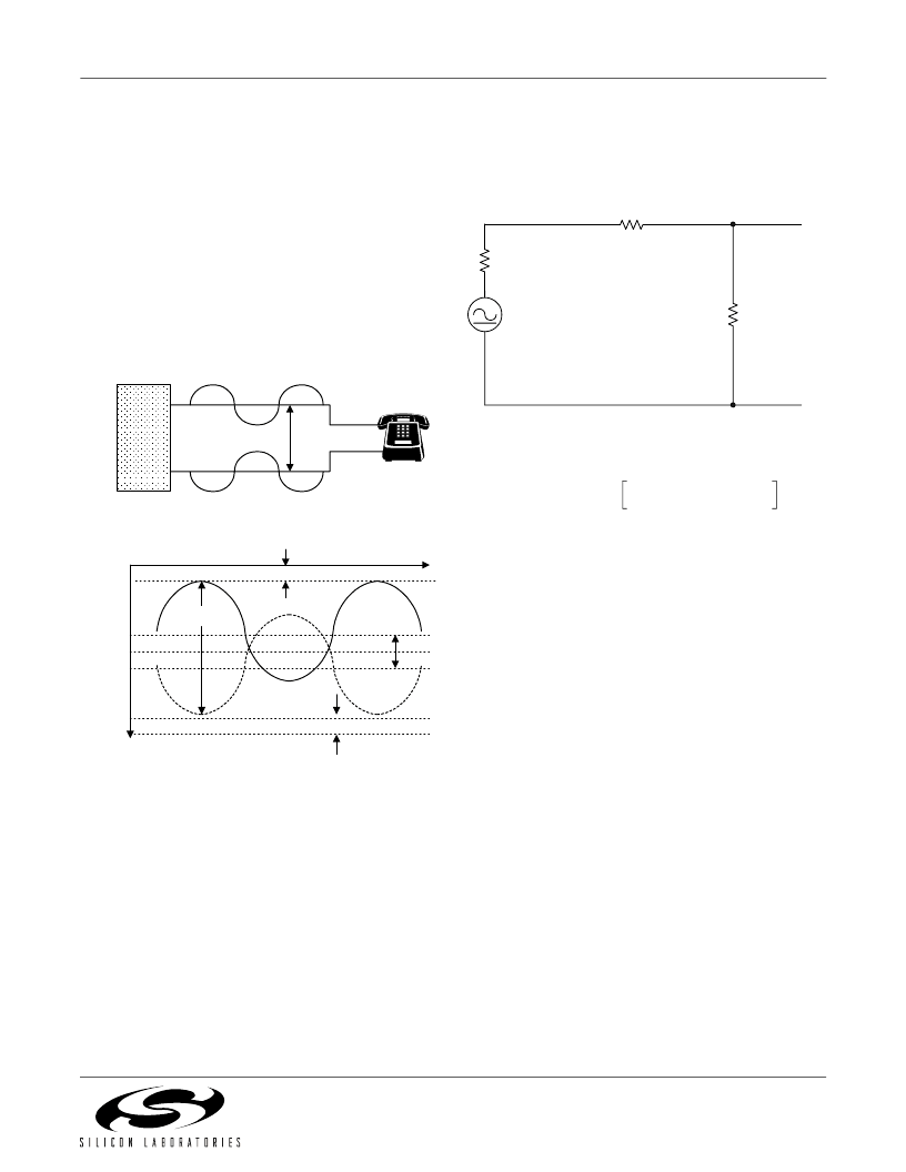
4.6. Ringing Generation
The Si3232 is designed to provide a balanced ringing
waveform with or without dc offset. The ringing
frequency, cadence, waveshape, and dc offset are all
register-programmable.
Using a balanced ringing scheme, the ringing signal is
applied to both the TIP and the RING lines using ringing
waveforms that are 180° out of phase with each other.
The resulting ringing signal seen across TIP-RING is
twice the amplitude of the ringing waveform on either
the TIP or the RING line, which allows the ringing
circuitry to withstand only half the total ringing amplitude
seen across TIP-RING.
Figure 16. Balanced Ringing Waveform and
Components
The purpose of an internal ringing scheme is to provide
>40 V
rms
into a 5 REN load at the terminal equipment
using a user-provided ringing battery supply. The
specific ringing supply voltage required depends on the
ringing voltage desired.
The ringing amplitude at the terminal equipment
depends on the loop impedance as well as the load
impedance in REN. The following equation can be used
to determine the TIP-RING ringing amplitude required
for a specific load and loop condition.
Figure 17. Simplified Loop Circuit During
Ringing
where
When ringing longer loop lengths, adding a dc offset
voltage is necessary to reliably detect a ring trip
condition (off-hook phone). Adding dc offset to the
ringing signal decreases the maximum possible ringing
amplitude. Adding significant dc offset also increases
the power dissipation in the Si3200 and may require
additional airflow or a modified PCB layout to maintain
acceptable operating temperatures. The Si3232
automatically applies and removes the ringing signal
during V
OC
-crossing periods to reduce noise and
crosstalk to adjacent lines. Table 23 provides a list of
registers required for internal ringing generation.
RING
TIP
V
RING
V
TIP
SLIC
V
OFF
GND
V
TIP
V
RING
V
BATH
V
PK
V
OV
V
CM
V
OFF
R
LOOP
V
RING
R
LOAD
V
TERM
+
–
R
OUT
V
TERM
V
RING
R
R
LOOP
R
LOAD
R
OUT
+
+
----------------------------------------------------------------
×
=
R
LOOP
0.09
per foot for 26 AWG wire
=
R
OUT
320
=
R
LOAD
#
REN
-------------------
=
相關PDF資料 |
PDF描述 |
|---|---|
| SI3211 | PROSLIC PROGRAMMABLE CMOS SLIC/CODEC WITH RINGING/BATTERY VOLTAGE GENERATION |
| SI3210M-KT | PROSLIC PROGRAMMABLE CMOS SLIC/CODEC WITH RINGING/BATTERY VOLTAGE GENERATION |
| SI3210M-BT | PROSLIC PROGRAMMABLE CMOS SLIC/CODEC WITH RINGING/BATTERY VOLTAGE GENERATION |
| SI3210 | PROSLIC PROGRAMMABLE CMOS SLIC/CODEC WITH RINGING/BATTERY VOLTAGE GENERATION |
| SI3210-BT | PROSLIC PROGRAMMABLE CMOS SLIC/CODEC WITH RINGING/BATTERY VOLTAGE GENERATION |
相關代理商/技術參數 |
參數描述 |
|---|---|
| SI3233 | 制造商:SILABS 制造商全稱:SILABS 功能描述:PROSLIC㈢ PROGRAMMABLE CMOS SLIC WITH RINGING/BATTERY VOLTAGE GENERATION |
| Si3233-C-FM | 功能描述:射頻無線雜項 Single-Chan SLIC RoHS:否 制造商:Texas Instruments 工作頻率:112 kHz to 205 kHz 電源電壓-最大:3.6 V 電源電壓-最小:3 V 電源電流:8 mA 最大功率耗散: 工作溫度范圍:- 40 C to + 110 C 封裝 / 箱體:VQFN-48 封裝:Reel |
| SI3233-C-FMR | 功能描述:電信線路管理 IC Single-CH SLIC only BJT/inductor dc-dc RoHS:否 制造商:STMicroelectronics 產品:PHY 接口類型:UART 電源電壓-最大:18 V 電源電壓-最小:8 V 電源電流:30 mA 最大工作溫度:+ 85 C 最小工作溫度:- 40 C 安裝風格:SMD/SMT 封裝 / 箱體:VFQFPN-48 封裝:Tray |
| SI3233M-X-FM | 制造商:SILABS 制造商全稱:SILABS 功能描述:PROSLIC㈢ PROGRAMMABLE CMOS SLIC WITH RINGING/BATTERY VOLTAGE GENERATION |
| SI3233M-X-GM | 制造商:SILABS 制造商全稱:SILABS 功能描述:PROSLIC㈢ PROGRAMMABLE CMOS SLIC WITH RINGING/BATTERY VOLTAGE GENERATION |
發(fā)布緊急采購,3分鐘左右您將得到回復。