- 您現(xiàn)在的位置:買賣IC網(wǎng) > PDF目錄192292 > S1M8660AX01-F0T0 SPECIALTY TELECOM CIRCUIT, CBCC48 PDF資料下載
參數(shù)資料
| 型號(hào): | S1M8660AX01-F0T0 |
| 元件分類: | 通信及網(wǎng)絡(luò) |
| 英文描述: | SPECIALTY TELECOM CIRCUIT, CBCC48 |
| 封裝: | 7 X 7 MM, BCC-48 |
| 文件頁(yè)數(shù): | 27/32頁(yè) |
| 文件大?。?/td> | 270K |
| 代理商: | S1M8660AX01-F0T0 |
第1頁(yè)第2頁(yè)第3頁(yè)第4頁(yè)第5頁(yè)第6頁(yè)第7頁(yè)第8頁(yè)第9頁(yè)第10頁(yè)第11頁(yè)第12頁(yè)第13頁(yè)第14頁(yè)第15頁(yè)第16頁(yè)第17頁(yè)第18頁(yè)第19頁(yè)第20頁(yè)第21頁(yè)第22頁(yè)第23頁(yè)第24頁(yè)第25頁(yè)第26頁(yè)當(dāng)前第27頁(yè)第28頁(yè)第29頁(yè)第30頁(yè)第31頁(yè)第32頁(yè)
S1M8660A (Preliminary)
RX IF/BBA WITH GPS
4
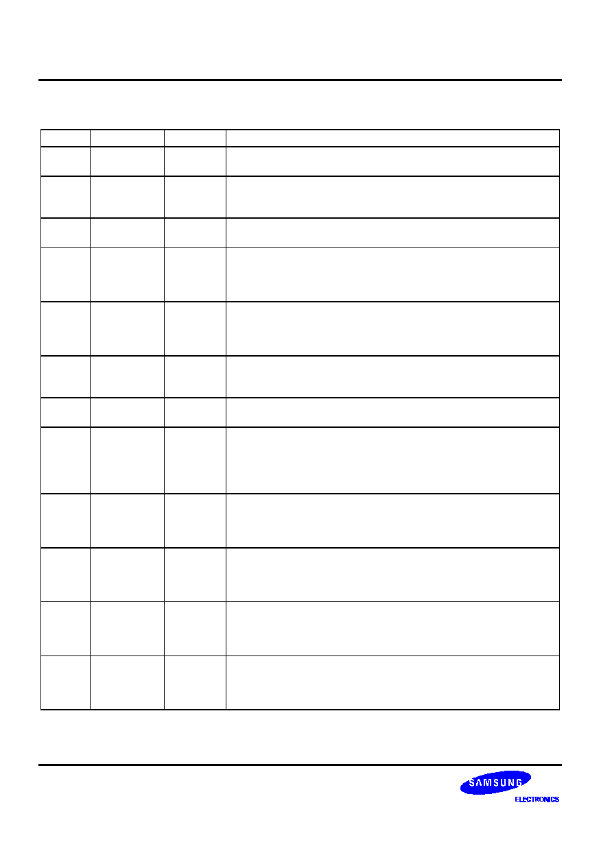
PIN DESCRIPTION
Pin No
Symbol
I/O
Description
1
FMCLK
SEN
FM ADC clock input ,received from the modem.
Signal frequency is 360kHz; if unconnected, it becomes LOW.
2
FMSTB
DI
FM STROBE input. Signal that controls the FM ADC initialization and
A-D conversion start. CLOCK frequency is 40kHz, which is received
from the MODEM; if unconnected, it remains at LOW.
7
RAGC_CONT
AI
AGC gain control input. The input voltage is allowed up to VDDA.
It remains at High impedance during SLEEP.
9
10
F/GRX_IF1
F/GRX_IF2
AI
FM/GPS IF input terminals, which have an input impedance of about
865
; generally, the FM IF SAW filter is connected to them. Usually,
the IF SAW output is single-ended.
When these terminals are not used, they remain at High impedance.
11
12
CRX_IF1
CRX_IF2
AI
CDMA IF input terminals, which have an input impedance of about
865
; generally, the CDMA IF SAW filter is connected to them.
Usually, the IF SAW output is differential. When these terminals are
not used, they remain at High impedance.
21
22
RXVCO_T1
RXVCO_T2
AI
Very sensitive terminal, which is connected to the oscillation L-C
resonance circuit.
Their impedance are about 2k
25
RXVCO_OUT
AO
Output for the PLL, able to output about -12dBm.
When this is not used, it remains at high impedance.
26
SEN
D
Input that permits/not permits SPI BUS control.
If the input is high, SPI control is allowed, and its related 3-pins, STB,
DATA, and CLK, perform their functions; if Low, related 3-pins,
IDLEB, FMB, and SLEEPB, are allowed to perform parallel control.
When this is not used, it remains at Low.
27
28
Q_OFS
I_OFS
AI
Control DC input for removing the DC offset generated in the
S1M8660A and system during CDMA and AMPS Mode. The control
DC is generated in the modem in PDM form, passes through the R-C
filter and is converted to DC, which is sent to this input terminal.
29
SLOTB
DI
This pin becomes Low during CDMA SLEEP Mode or FM RX Mode,
the system is assumed to be in the Rx SLOT mode, and all functions
are stopped except for the VCO, VCO buffer and TCXO/N. No
external clock inputs are not required in this product with this function.
30
IDLEB/STB
DI
When SEN is high, this pin becomes the STROBE input with the
permit of the 3-LINE Serial control input.
When SEN is low, parallel control input is allowed and this pin
executes the IDLEB function. If this pin is opened, it remains at Low.
31
FMB/DATA
BI
When SEN is high, this pin inputs and outputs data with the permit of
the 3-line serial control input. When SEN is low, parallel control input
is allowed and this pin performs IDLEB. If this pin is opened, it
remains at Low.
相關(guān)PDF資料 |
PDF描述 |
|---|---|
| S1M8836X01-G0T0 | PLL FREQUENCY SYNTHESIZER, 1000 MHz, CQCC24 |
| S1P-SLV | 1 CONTACT(S), FEMALE, TWO PART BOARD CONNECTOR, CRIMP |
| S1T0567X01-D0B0 | TELECOM, TONE DECODER CIRCUIT, PDIP8 |
| S1U2-12-RC | 500 MHz - 2000 MHz RF/MICROWAVE SGL POLE SGL THROW SWITCH, 1.5 dB INSERTION LOSS |
| S2004VS2 | 4 A, 200 V, SCR, TO-251 |
相關(guān)代理商/技術(shù)參數(shù) |
參數(shù)描述 |
|---|---|
| S1M8662A | 制造商:SAMSUNG 制造商全稱:Samsung semiconductor 功能描述:CDMA/PCS/GPS Triple Mode IF/ baseband IC |
| S1M8662AX01-F0T0 | 制造商:SAMSUNG 制造商全稱:Samsung semiconductor 功能描述:CDMA/PCS/GPS Triple Mode IF/ baseband IC |
| S1M8821 | 制造商:SAMSUNG 制造商全稱:Samsung semiconductor 功能描述:INTERGER RF/IF DUAL PLL |
| S1M8821X01-R0T0 | 制造商:SAMSUNG 制造商全稱:Samsung semiconductor 功能描述:INTERGER RF/IF DUAL PLL |
| S1M8822 | 制造商:SAMSUNG 制造商全稱:Samsung semiconductor 功能描述:INTERGER RF/IF DUAL PLL |
發(fā)布緊急采購(gòu),3分鐘左右您將得到回復(fù)。