- 您現(xiàn)在的位置:買賣IC網(wǎng) > PDF目錄230917 > RDC-19220-493K (DATA DEVICE CORP) SYNCHRO OR RESOLVER TO DIGITAL CONVERTER, CDIP40 PDF資料下載
參數(shù)資料
| 型號: | RDC-19220-493K |
| 廠商: | DATA DEVICE CORP |
| 元件分類: | 位置變換器 |
| 英文描述: | SYNCHRO OR RESOLVER TO DIGITAL CONVERTER, CDIP40 |
| 封裝: | CERAMIC, DDIP-40 |
| 文件頁數(shù): | 18/22頁 |
| 文件大小: | 304K |
| 代理商: | RDC-19220-493K |
5
Data Device Corporation
www.ddc-web.com
RDC-19220 SERIES
N-09/03-0
are done with external resistors and capacitors so that the con-
verter loop dynamics can be easily controlled by the user.
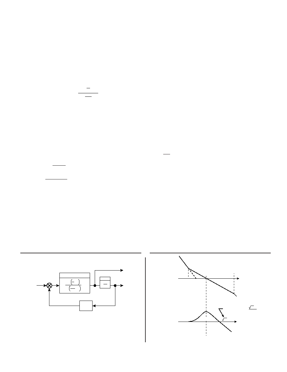
TRANSFER FUNCTION AND BODE PLOT
The dynamic performance of the converter can be determined from
its Transfer Function Block Diagrams and its Bode Plots (open and
closed loop). These are shown in FIGURES 2, 3, and 4.
The open loop transfer function is as follows:
where A is the gain coefficient and A2= A1A2
and B is the frequency of lead compensation.
The components of gain coefficient are error gradient, integrator
gain and VCO gain. These can be broken down as follows:
RV, RB, and CBW are selected by the user to set velocity scaling
and bandwidth.
GENERAL SETUP CONSIDERATIONS
Note: For detailed application and technical information see the RDC-19220 & RD-
19230 series converter applications manual (Document number MN-19220XX-001)
which is available for download from the DDC web site @ WWW.DDC-WEB.COM.
- Error Gradient = 0.011 volts per LSB (CT + Error Amp + Demod
with 2 Vrms input)
- Integrator Gain =
volts per second per volt
- VCO Gain =
LSBs per second per volt
where: Cs = 10 pF
Fs = 67 kHz when Rs = 30 k
Fs = 100 kHz when Rs = 20 k
Fs = 134 kHz when Rs = 15 k
CVCO = 50 pF
Cs Fs
1.1 CBW
1
1.25 RV CVCO
2
S
A
+1
(
)
B
2
S
+1
(
)
10B
Open Loop Transfer Function =
ERROR PROCESSOR
RESOLVER
INPUT
(
θ)
VELOCITY
OUT
DIGITAL
POSITION
OUT (
φ)
VCO
CT
S
A
+ 1
1
B
S
+ 1
10B
H = 1
+
-
e
A2
S
-12
db/oct
BA
2A
-6 db/oct
10B
ω (rad/sec)
2A
2 2 A
ω (rad/sec)
f
= BW (Hz) =
BW
2 A
π
CLOSED LOOP
(B = A/2)
GAIN = 0.4
GAIN = 4
(CRITICALLY DAMPED)
OPEN LOOP
FIGURE 3. TRANSFER FUNCTION
BLOCK DIAGRAM #2
FIGURE 4. BODE PLOTS
DDC has external component selection software which consid-
ers all the criteria below, and in a simple fashion, asks the key
parameters (carrier frequency, resolution, bandwidth, and track-
ing rate) to derive the external component value.
The following recommendations should be considered when
installing the RDC-19220 Series R/D converters:
1) In setting the bandwidth (BW) and Tracking Rate (TR) (select-
ing five external components), the system requirements need
to be considered. For greatest noise immunity, select the min-
imum BW and TR the system will allow.
2) Power supplies are ±5 V dc. For lowest noise performance it
is recommended that a 0.1 F or larger cap be connected
from each supply to ground near the converter package.
3) Resolver inputs and velocity output are referenced to A GND.
This pin should be connected to GND near the converter
package. Digital currents flowing through ground will not dis-
turb the analog signals.
4) The BIT output which is active low is activated by an error of
approximately 100 LSBs. During normal operation for step
inputs or on power up, a large error can exist.
5) This device has several high impedance amplifier inputs (+C,
-C, +S, -S, -VCO and -VSUM). These nodes are sensitive to
noise and coupling components should be connected as
close as possible.
6) Setup of bandwidth and velocity scaling for the optimized crit-
ically damped case should proceed as follows:
相關(guān)PDF資料 |
PDF描述 |
|---|---|
| RD-14597D1-345 | SYNCHRO OR RESOLVER TO DIGITAL CONVERTER, DIP36 |
| RD-14597D1-355K | SYNCHRO OR RESOLVER TO DIGITAL CONVERTER, DIP36 |
| RD-14597D1-295S | SYNCHRO OR RESOLVER TO DIGITAL CONVERTER, DIP36 |
| RD-14590D1-184 | SYNCHRO OR RESOLVER TO DIGITAL CONVERTER, MDMA36 |
| RDC-361-M-1 | SYNCHRO OR RESOLVER TO DIGITAL CONVERTER, DIP34 |
相關(guān)代理商/技術(shù)參數(shù) |
參數(shù)描述 |
|---|---|
| RDC-19220S | 制造商:未知廠家 制造商全稱:未知廠家 功能描述:Resolver and Synchro To Digital Converters |
| RDC-19220S-102 | 制造商:未知廠家 制造商全稱:未知廠家 功能描述:LVDT/Resolver-to-Digital Converter |
| RDC-19220S-103 | 制造商:未知廠家 制造商全稱:未知廠家 功能描述:LVDT/Resolver-to-Digital Converter |
| RDC-19220S-112 | 制造商:未知廠家 制造商全稱:未知廠家 功能描述:LVDT/Resolver-to-Digital Converter |
| RDC-19220S-113 | 制造商:未知廠家 制造商全稱:未知廠家 功能描述:LVDT/Resolver-to-Digital Converter |
發(fā)布緊急采購,3分鐘左右您將得到回復(fù)。