- 您現(xiàn)在的位置:買賣IC網(wǎng) > PDF目錄296941 > QL8150-6PFN144C (QUICKLOGIC CORP) FPGA, 640 CLBS, 188946 GATES, PQFP144 PDF資料下載
參數(shù)資料
| 型號: | QL8150-6PFN144C |
| 廠商: | QUICKLOGIC CORP |
| 元件分類: | FPGA |
| 英文描述: | FPGA, 640 CLBS, 188946 GATES, PQFP144 |
| 封裝: | LEAD FREE, TQFP-144 |
| 文件頁數(shù): | 23/96頁 |
| 文件大小: | 1607K |
| 代理商: | QL8150-6PFN144C |
第1頁第2頁第3頁第4頁第5頁第6頁第7頁第8頁第9頁第10頁第11頁第12頁第13頁第14頁第15頁第16頁第17頁第18頁第19頁第20頁第21頁第22頁當前第23頁第24頁第25頁第26頁第27頁第28頁第29頁第30頁第31頁第32頁第33頁第34頁第35頁第36頁第37頁第38頁第39頁第40頁第41頁第42頁第43頁第44頁第45頁第46頁第47頁第48頁第49頁第50頁第51頁第52頁第53頁第54頁第55頁第56頁第57頁第58頁第59頁第60頁第61頁第62頁第63頁第64頁第65頁第66頁第67頁第68頁第69頁第70頁第71頁第72頁第73頁第74頁第75頁第76頁第77頁第78頁第79頁第80頁第81頁第82頁第83頁第84頁第85頁第86頁第87頁第88頁第89頁第90頁第91頁第92頁第93頁第94頁第95頁第96頁
2007 QuickLogic Corporation
Eclipse II Family Data Sheet Rev. Q
3
Programmable Logic Architectural Overview
The Eclipse II logic cell structure is presented in Figure 2. This architectural feature addresses today's register-
intensive designs.
The Eclipse II logic cell structure presented in Figure 2 is a dual register, multiplexer-based logic cell. It is
designed for wide fan-in and multiple, simultaneous output functions. Both registers share CLK, SET, and
RESET inputs. The second register has a two-to-one multiplexer controlling its input. The register can be
loaded from the NZ output or directly from a dedicated input.
NOTE: The input PP is not an “input” in the classical sense. It is a static input to the logic cell and selects
which path (NZ or PS) is used as an input to the Q2Z register. All other inputs are dynamic and can
be connected to multiple routing channels.
The complete logic cell consists of two six-input AND gates, four two-input AND gates, seven two-to-one
multiplexers, and two D flip-flops with asynchronous SET and RESET controls. The cell has a fan-in of 30
(including register control lines), fits a wide range of functions with up to 17 simultaneous inputs, and has six
outputs (four combinatorial and two registered). The high logic capacity and fan-in of the logic cell
accommodates many user functions with a single level of logic delay while other architectures require two or
more levels of delay.
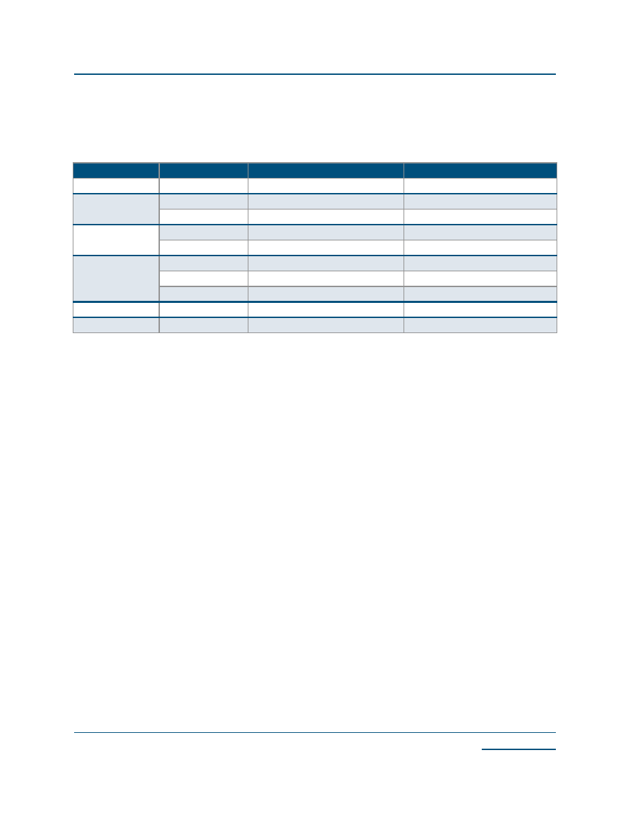
Table 3: Performance Standards
Function
Description
Slowest Speed Grade
Fastest Speed Grade
Multiplexer
16:1
2.8 ns
2.4 ns
Parity Tree
24
3.4 ns
2.9 ns
36
4.6 ns
3.9 ns
Counter
16 bit
275 MHz
328 MHz
32 bit
250 MHz
300 MHz
FIFO
128 x 32
197 MHz
235 MHz
128 x 64
188 MHz
266 MHz
256 x 16
208 MHz
248 MHz
Clock-to-Out
4 ns
3.3 ns
System clock
200 MHz
300 MHz
相關(guān)PDF資料 |
PDF描述 |
|---|---|
| QL8150-6PFN144I | FPGA, 640 CLBS, 188946 GATES, PQFP144 |
| QL8150-6PFN144M | FPGA, 640 CLBS, 188946 GATES, PQFP144 |
| QL8150-7PFN144C | FPGA, 640 CLBS, 188946 GATES, PQFP144 |
| QL8150-7PFN144I | FPGA, 640 CLBS, 188946 GATES, PQFP144 |
| QL8150-7PFN144M | FPGA, 640 CLBS, 188946 GATES, PQFP144 |
相關(guān)代理商/技術(shù)參數(shù) |
參數(shù)描述 |
|---|---|
| QL8250 | 制造商:未知廠家 制造商全稱:未知廠家 功能描述:LOW POWER FPGA COMBINING PERFORMANCE DENSITY AND EMBEDED RAM |
| QL8250-6PQN208C-5690 | 制造商:QuickLogic Corporation 功能描述: |
| QL8250-6PQN208C-5691 | 制造商:QuickLogic Corporation 功能描述: |
| QL82SD | 制造商:未知廠家 制造商全稱:未知廠家 功能描述:10 High Speed Bus LVDS Serial Links bandwidth up to 5 Gbps |
| QL82SD-PB516 | 制造商:未知廠家 制造商全稱:未知廠家 功能描述:10 High Speed Bus LVDS Serial Links bandwidth up to 5 Gbps |
發(fā)布緊急采購,3分鐘左右您將得到回復。