- 您現在的位置:買賣IC網 > PDF目錄385747 > PSD813F2A (意法半導體) Flash In-System Programmable(ISP) Peripherals For 8-bit MCUs(用于八位MCU的閃速在系統(tǒng)可編程外圍芯片) PDF資料下載
參數資料
| 型號: | PSD813F2A |
| 廠商: | 意法半導體 |
| 英文描述: | Flash In-System Programmable(ISP) Peripherals For 8-bit MCUs(用于八位MCU的閃速在系統(tǒng)可編程外圍芯片) |
| 中文描述: | Flash在系統(tǒng)可編程(ISP)為周邊8位微控制器(用于八位微控制器的閃速在系統(tǒng)可編程外圍芯片) |
| 文件頁數: | 16/103頁 |
| 文件大小: | 1180K |
| 代理商: | PSD813F2A |
第1頁第2頁第3頁第4頁第5頁第6頁第7頁第8頁第9頁第10頁第11頁第12頁第13頁第14頁第15頁當前第16頁第17頁第18頁第19頁第20頁第21頁第22頁第23頁第24頁第25頁第26頁第27頁第28頁第29頁第30頁第31頁第32頁第33頁第34頁第35頁第36頁第37頁第38頁第39頁第40頁第41頁第42頁第43頁第44頁第45頁第46頁第47頁第48頁第49頁第50頁第51頁第52頁第53頁第54頁第55頁第56頁第57頁第58頁第59頁第60頁第61頁第62頁第63頁第64頁第65頁第66頁第67頁第68頁第69頁第70頁第71頁第72頁第73頁第74頁第75頁第76頁第77頁第78頁第79頁第80頁第81頁第82頁第83頁第84頁第85頁第86頁第87頁第88頁第89頁第90頁第91頁第92頁第93頁第94頁第95頁第96頁第97頁第98頁第99頁第100頁第101頁第102頁第103頁
PSD8XXF2/3/4/5
16/103
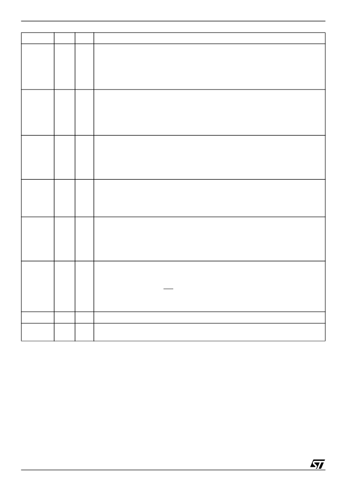
Note: 1. The pin numbers in this table are for the PLCC package only. See the package information, on page 98 onwards, for pin numbers
on other package types.
2. These functions can be multiplexed with other functions.
PSD8XXFX REGISTER DESCRIPTION AND ADDRESS OFFSET
Table 7 shows the offset addresses to the
PSD8XXFX registers relative to the CSIOP base
address. The CSIOP space is the 256 bytes of ad-
dress that is allocated by the user to the internal
PSD8XXFX registers. Table 7 provides brief de-
scriptions of the registers in CSIOP space. The fol-
lowing section gives a more detailed description.
PC5
13
I/O
PC5 pin of Port C. This port pin can be configured to have the following functions:
1. MCU I/O – write to or read from a standard output or input port.
2. CPLD macrocell (McellBC5) output.
3. Input to the PLDs.
4. TDI input
2
for the JTAG Serial Interface.
This pin can be configured as a CMOS or Open Drain output.
PC6
12
I/O
PC6 pin of Port C. This port pin can be configured to have the following functions:
1. MCU I/O – write to or read from a standard output or input port.
2. CPLD macrocell (McellBC6) output.
3. Input to the PLDs.
4. TDO output
2
for the JTAG Serial Interface.
This pin can be configured as a CMOS or Open Drain output.
PC7
11
I/O
PC7 pin of Port C. This port pin can be configured to have the following functions:
1. MCU I/O – write to or read from a standard output or input port.
2. CPLD macrocell (McellBC7) output.
3. Input to the PLDs.
4. DBE – active Low Data Byte Enable input from 68HC912 type MCUs.
This pin can be configured as a CMOS or Open Drain output.
PD0
10
I/O
PD0 pin of Port D. This port pin can be configured to have the following functions:
1. ALE/AS input latches address output from the MCU.
2. MCU I/O – write or read from a standard output or input port.
3. Input to the PLDs.
4. CPLD output (External Chip Select).
PD1
9
I/O
PD1 pin of Port D. This port pin can be configured to have the following functions:
1. MCU I/O – write to or read from a standard output or input port.
2. Input to the PLDs.
3. CPLD output (External Chip Select).
4. CLKIN – clock input to the CPLD macrocells, the APD Unit’s Power-down counter, and
the CPLD AND Array.
PD2
8
I/O
PD2 pin of Port D. This port pin can be configured to have the following functions:
1. MCU I/O
–
write to or read from a standard output or input port.
2. Input to the PLDs.
3. CPLD output (External Chip Select).
4. PSD Chip Select Input (CSI). When Low, the MCU can access the PSD8XXFX
memory and I/O. When High, the PSD8XXFX memory blocks are disabled to conserve
power.
V
CC
15, 38
Supply Voltage
GND
1, 16,
26
Ground pins
Pin Name
Pin
Type
Description
相關PDF資料 |
PDF描述 |
|---|---|
| PSD813F2V | Flash In-System Programmable (ISP) Peripherals for8-bits MCUs, 3V |
| PSD813F2V-15J1T | Flash In-System Programmable (ISP) Peripherals for8-bits MCUs, 3V |
| PSD833F2V | Flash In-System Programmable (ISP) Peripherals for8-bits MCUs, 3V |
| PSD833F2V-15J1T | Flash In-System Programmable (ISP) Peripherals for8-bits MCUs, 3V |
| PSD853F2V | Flash In-System Programmable (ISP) Peripherals for8-bits MCUs, 3V |
相關代理商/技術參數 |
參數描述 |
|---|---|
| PSD813F2A-12J | 制造商:STMICROELECTRONICS 制造商全稱:STMicroelectronics 功能描述:Flash In-System Programmable ISP Peripherals For 8-bit MCUs |
| PSD813F2A-12JI | 制造商:STMICROELECTRONICS 制造商全稱:STMicroelectronics 功能描述:Flash In-System Programmable ISP Peripherals For 8-bit MCUs |
| PSD813F2A-12JIT | 制造商:STMICROELECTRONICS 制造商全稱:STMicroelectronics 功能描述:Flash In-System Programmable ISP Peripherals For 8-bit MCUs |
| PSD813F2A-12JT | 制造商:STMICROELECTRONICS 制造商全稱:STMicroelectronics 功能描述:Flash In-System Programmable ISP Peripherals For 8-bit MCUs |
| PSD813F2A-12M | 制造商:STMICROELECTRONICS 制造商全稱:STMicroelectronics 功能描述:Flash In-System Programmable ISP Peripherals For 8-bit MCUs |
發(fā)布緊急采購,3分鐘左右您將得到回復。