- 您現(xiàn)在的位置:買賣IC網(wǎng) > PDF目錄368225 > PSD4235F2-20MI (意法半導(dǎo)體) Flash In-System Programmable ISP Peripherals For 16-bit MCUs 5V Supply PDF資料下載
參數(shù)資料
| 型號: | PSD4235F2-20MI |
| 廠商: | 意法半導(dǎo)體 |
| 英文描述: | Flash In-System Programmable ISP Peripherals For 16-bit MCUs 5V Supply |
| 中文描述: | Flash在系統(tǒng)可編程ISP的外設(shè)的16位微控制器5V電源 |
| 文件頁數(shù): | 61/89頁 |
| 文件大?。?/td> | 703K |
| 代理商: | PSD4235F2-20MI |
第1頁第2頁第3頁第4頁第5頁第6頁第7頁第8頁第9頁第10頁第11頁第12頁第13頁第14頁第15頁第16頁第17頁第18頁第19頁第20頁第21頁第22頁第23頁第24頁第25頁第26頁第27頁第28頁第29頁第30頁第31頁第32頁第33頁第34頁第35頁第36頁第37頁第38頁第39頁第40頁第41頁第42頁第43頁第44頁第45頁第46頁第47頁第48頁第49頁第50頁第51頁第52頁第53頁第54頁第55頁第56頁第57頁第58頁第59頁第60頁當(dāng)前第61頁第62頁第63頁第64頁第65頁第66頁第67頁第68頁第69頁第70頁第71頁第72頁第73頁第74頁第75頁第76頁第77頁第78頁第79頁第80頁第81頁第82頁第83頁第84頁第85頁第86頁第87頁第88頁第89頁
61/89
PSD4235G2
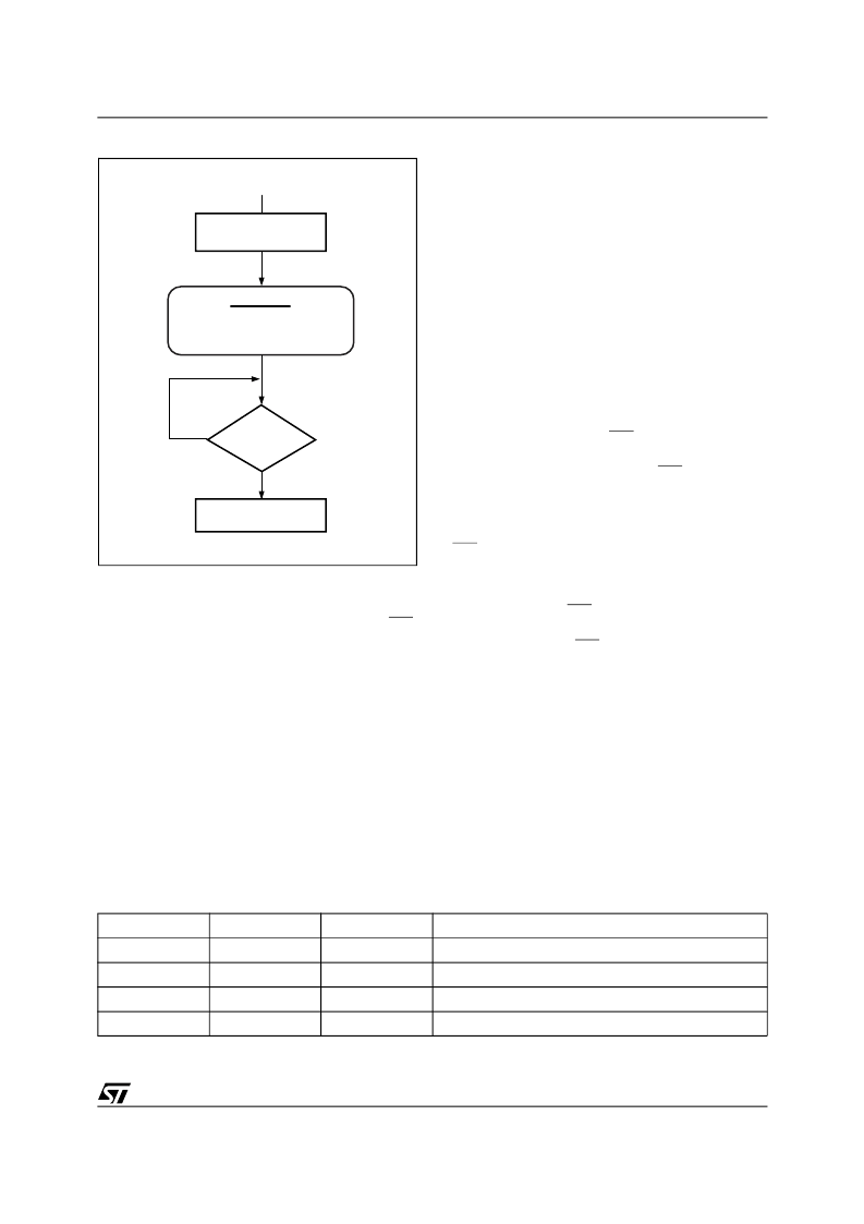
Figure 33. Enable Power-down Flow Chart
Other Power Saving Options.
The PSD offers
other reduced power saving options that are inde-
pendent of the Power-down mode. Except for the
SRAM Stand-by and PSD Chip Select Input (CSI,
PD2) features, they are enabled by setting bits in
PMMR0 and PMMR2 (as summarised in Table 23
and Table 24).
PLD Power Management
The power and speed of the PLDs are controlled
by the Turbo bit (bit 3) in PMMR0. By setting the
bit to 1, the Turbo mode is off and the PLDs con-
sume the specified Stand-by current when the in-
puts are not switching for an extended time of
70 ns. The propagation delay time is increased af-
ter the Turbo bit is set to 1 (turned off) when the in-
puts change at a composite frequency of less than
15 MHz. When the Turbo bit is reset to 0 (turned
on), the PLDs run at full power and speed. The
Turbo bit affects the PLD’s DC power, AC power,
and propagation delay. See the AC and DC char-
acteristics tables for PLD timing values (Table 67).
Blocking MCU control signals with the PMMR2 bits
can further reduce PLD AC power consumption.
SRAM Stand-by Mode (Battery Backup).
The
PSD supports a battery backup mode in which the
contents of the SRAM are retained in the event of
a power loss. The SRAM has Voltage Stand-by
(VSTBY, PE6) that can be connected to an exter-
nal battery. When V
CC
becomes lower than V
STBY
then the PSD automatically connects to Voltage
Stand-by (VSTBY, PE6) as a power source to the
SRAM. The SRAM Stand-by current (I
STBY
) is typ-
ically 0.5 μA. The SRAM data retention voltage is
2 V minimum. The Battery-on Indicator (VBATON)
can be routed to PE7. This signal indicates when
the V
CC
has dropped below V
STBY
, and that the
SRAM is running on battery power.
PSD Chip Select Input (CSI, PD2)
PD2 of Port D can be configured in PSDsoft Ex-
press as PSD Chip Select Input (CSI). When Low,
the signal selects and enables the internal primary
Flash memory, secondary Flash memory, SRAM,
and I/O blocks for Read or Write operations involv-
ing the PSD. A High on PSD Chip Select Input
(CSI, PD2) disables the primary Flash memory,
secondary Flash memory, and SRAM, and reduc-
es the PSD power consumption. However, the
PLD and I/O signals remain operational when PSD
Chip Select Input (CSI, PD2) is High.
There may be a timing penalty when using PSD
Chip Select Input (CSI, PD2) depending on the
speed grade of the PSD that you are using. See
the timing parameter t
SLQV
in Table 67.
Input Clock.
The PSD provides the option to turn
off CLKIN (PD1) to the PLD to save AC power con-
sumption. CLKIN (PD1) is an input to the PLD
AND Array and the Output Macrocells (OMC).
During Power-down mode, or, if CLKIN (PD1) is
not being used as part of the PLD logic equation,
the clock should be disabled to save AC power.
CLKIN (PD1) is disconnected from the PLD AND
Array or the Macrocells block by setting bits 4 or 5
to a 1 in PMMR0.
Table 50. APD Counter Operation
Enable APD
Set PMMR0 Bit 1 = 1
PSD in Power
Down Mode
ALE/AS idle
for 15 CLKIN
clocks
RESET
Yes
No
OPTIONAL
Disable desired inputs to PLD
by setting PMMR0 bits 4 and 5
and PMMR2 bits 0 to 6.
AI04940
APD Enable Bit
ALE PD Polarity
ALE Level
APD Counter
0
X
X
Not Counting
1
X
Pulsing
Not Counting
1
1
1
Counting (Generates PDN after 15 Clocks)
1
0
0
Counting (Generates PDN after 15 Clocks)
相關(guān)PDF資料 |
PDF描述 |
|---|---|
| PSD4235F2-20U | Flash In-System-Programmable Peripherals for 16-Bit MCUs |
| PSD4235F2-20UI | Flash In-System-Programmable Peripherals for 16-Bit MCUs |
| PSD4235F2-A-12M | Flash In-System-Programmable Peripherals for 16-Bit MCUs |
| PSD4235F2-A-12MI | Flash In-System-Programmable Peripherals for 16-Bit MCUs |
| PSD4235F2-A-12U | Flash In-System-Programmable Peripherals for 16-Bit MCUs |
相關(guān)代理商/技術(shù)參數(shù) |
參數(shù)描述 |
|---|---|
| PSD4235G2-70U | 功能描述:SPLD - 簡單可編程邏輯器件 5.0V 4M 70ns RoHS:否 制造商:Texas Instruments 邏輯系列:TICPAL22V10Z 大電池數(shù)量:10 最大工作頻率:66 MHz 延遲時間:25 ns 工作電源電壓:4.75 V to 5.25 V 電源電流:100 uA 最大工作溫度:+ 75 C 最小工作溫度:0 C 安裝風(fēng)格:Through Hole 封裝 / 箱體:DIP-24 |
| PSD4235G2-90U | 功能描述:CPLD - 復(fù)雜可編程邏輯器件 5.0V 4M 90ns RoHS:否 制造商:Lattice 系列: 存儲類型:EEPROM 大電池數(shù)量:128 最大工作頻率:333 MHz 延遲時間:2.7 ns 可編程輸入/輸出端數(shù)量:64 工作電源電壓:3.3 V 最大工作溫度:+ 90 C 最小工作溫度:0 C 封裝 / 箱體:TQFP-100 |
| PSD4235G2-90UI | 功能描述:CPLD - 復(fù)雜可編程邏輯器件 5.0V 4M 90ns RoHS:否 制造商:Lattice 系列: 存儲類型:EEPROM 大電池數(shù)量:128 最大工作頻率:333 MHz 延遲時間:2.7 ns 可編程輸入/輸出端數(shù)量:64 工作電源電壓:3.3 V 最大工作溫度:+ 90 C 最小工作溫度:0 C 封裝 / 箱體:TQFP-100 |
| PSD4235G2V-12UI | 功能描述:CPLD - 復(fù)雜可編程邏輯器件 3.3V 4M 120ns RoHS:否 制造商:Lattice 系列: 存儲類型:EEPROM 大電池數(shù)量:128 最大工作頻率:333 MHz 延遲時間:2.7 ns 可編程輸入/輸出端數(shù)量:64 工作電源電壓:3.3 V 最大工作溫度:+ 90 C 最小工作溫度:0 C 封裝 / 箱體:TQFP-100 |
| PSD4235G2V-90U | 功能描述:CPLD - 復(fù)雜可編程邏輯器件 3.3V 4M 90ns RoHS:否 制造商:Lattice 系列: 存儲類型:EEPROM 大電池數(shù)量:128 最大工作頻率:333 MHz 延遲時間:2.7 ns 可編程輸入/輸出端數(shù)量:64 工作電源電壓:3.3 V 最大工作溫度:+ 90 C 最小工作溫度:0 C 封裝 / 箱體:TQFP-100 |
發(fā)布緊急采購,3分鐘左右您將得到回復(fù)。