- 您現在的位置:買賣IC網 > PDF目錄378055 > PM5384 (PMC-Sierra, Inc.) Single Channel OC-3c ATM and POS Physical Layer Device PDF資料下載
參數資料
| 型號: | PM5384 |
| 廠商: | PMC-Sierra, Inc. |
| 英文描述: | Single Channel OC-3c ATM and POS Physical Layer Device |
| 中文描述: | 單信道OC - 3C型自動柜員機和POS物理層設備 |
| 文件頁數: | 1/2頁 |
| 文件大小: | 46K |
| 代理商: | PM5384 |
PM5384
Advance
Single Channel OC-3c ATM and POS Physical Layer Device
S/UNI-1x155
PMC-2011690 (A1)
PROPRIETARY AND CONFIDENTIAL TO PMC
-
SIERRA, INC., AND FOR ITS CUSTOMERS
’
INTERNAL USE
Copyright PMC
-
Sierra, Inc. 2001.
FEATURES
Single chip ATM and Packet over
SONET/SDH Physical Layer Device
operating at 155.52 Mbit/s.
Implements the ATM Forum User
Network Interface (UNI) and the ATM
physical layer for Broadband ISDN
according to CCITT Recommendation
I.432.
Implements Point-to-Point Protocol
(PPP) over SONET/SDH according to
RFC 2615.
Processes duplex bit-serial 155.52
Mbit/s STS-3c/STM-1 data streams
with on-chip clock and data recovery
and clock synthesis.
Complies with Bellcore GR-253-CORE
(1995 Issue) jitter tolerance, jitter
transfer and intrinsic jitter criteria.
Provides control circuitry required to
comply with Bellcore GR-253-CORE
WAN clocking requirements related to
wander transfer, holdover and long
term stability when using an external
VCXO.
Provides a UTOPIA Level 2, 8-bit wide
system interface (clocked up to 52
MHz) with parity support for ATM
applications.
Provides a UTOPIA Level 2, 16-bit
wide system interface (clocked up to
52 MHz) with parity support for ATM
applications.
Provides a SATURN POS-PHY Level
2, 16-bit system interface (clocked up
to 52 MHz) for Packet over
SONET/SDH (POS) applications
(similar to UTOPIA Level 2, but
adapted for packet transfer).
Provides support functions for 1+1
APS operation.
GENERAL
Provides a standard 5 signal IEEE
1149.1 JTAG test port for boundary
scan board test purposes.
Provides a generic 8-bit
microprocessor bus interface for
configuration, control and status
monitoring.
Low power 2.5/3.3 V CMOS with 5 V
TTL-compatible digital inputs/outputs
(PECL inputs/outputs are 3.3 V and
5 V compatible).
Industrial temperature range (-40
°
C to
+85
°
C).
15 mm x15 mm 196 pin stPBGA
package with 1 mm ball pitch.
APPLICATIONS
Routers and Layer 3 Switches.
3G Wireless Base Station Controllers.
DSLAM Uplinks.
WAN and Edge ATM switches.
LAN switches and hubs.
Packet switches and hubs.
Network Interface Cards and Uplinks.
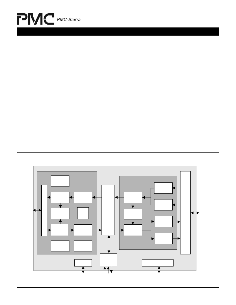
BLOCK DIAGRAM
External
APS
Interface
U
S
S
Rx
Line O/H
Processor
Tx
Line O/H
Processor
Tx
Section O/H
Processor
Section
Trace Buffer
Rx
Section O/H
Processor
WAN
Synch.
Sync Status,
BERM
Section/
Line DCC
Insertion
Section/
Line DCC
Extraction
P
A
Microprocessor Interface
Test Data
JTAG Test
Access Port
Rx
ATM Cell
Processor
Rx
POS Frame
Processor
Rx
Path O/H
Processor
Tx
Path O/H
Processor
Tx
POS Frame
Processor
Tx
ATM Cell
Processor
Path
Trace Buffer
155.52 Mbit/s
UTOPIA Level 1
8-bit x 52 MHz
UTOPIA Level 2
POS-PHY Level 2
16-bit x 52 MHz
16-bit
Microprocessor
Bus
A
A
A
相關PDF資料 |
PDF描述 |
|---|---|
| PM5389 | SONET/SDH Wideband Cross-Connect |
| PM5390 | CONNECTOR |
| PM5392 | SATURN User Network Interface for 9.953 Gbit/s |
| PM5945-UTP5 | ATM PHYSICAL INTERFACE APPLICATION BOARD FOR CAT-5 UTP |
| PM5945 | CONN |
相關代理商/技術參數 |
參數描述 |
|---|---|
| PM5389 | 制造商:PMC 制造商全稱:PMC 功能描述:SONET/SDH Wideband Cross-Connect |
| PM5389FI | 制造商:PMC-Sierra 功能描述: |
| PM538D | 制造商:未知廠家 制造商全稱:未知廠家 功能描述:Analog IC |
| PM538DS | 制造商:未知廠家 制造商全稱:未知廠家 功能描述:Analog IC |
發(fā)布緊急采購,3分鐘左右您將得到回復。