- 您現(xiàn)在的位置:買賣IC網(wǎng) > PDF目錄368024 > PIC16C717 (Microchip Technology Inc.) 8-Bit CMOS Microcontrollers(8位CMOS微控制器) PDF資料下載
參數(shù)資料
| 型號: | PIC16C717 |
| 廠商: | Microchip Technology Inc. |
| 英文描述: | 8-Bit CMOS Microcontrollers(8位CMOS微控制器) |
| 中文描述: | 8位CMOS微控制器(8位的CMOS微控制器) |
| 文件頁數(shù): | 64/220頁 |
| 文件大小: | 3585K |
| 代理商: | PIC16C717 |
第1頁第2頁第3頁第4頁第5頁第6頁第7頁第8頁第9頁第10頁第11頁第12頁第13頁第14頁第15頁第16頁第17頁第18頁第19頁第20頁第21頁第22頁第23頁第24頁第25頁第26頁第27頁第28頁第29頁第30頁第31頁第32頁第33頁第34頁第35頁第36頁第37頁第38頁第39頁第40頁第41頁第42頁第43頁第44頁第45頁第46頁第47頁第48頁第49頁第50頁第51頁第52頁第53頁第54頁第55頁第56頁第57頁第58頁第59頁第60頁第61頁第62頁第63頁當前第64頁第65頁第66頁第67頁第68頁第69頁第70頁第71頁第72頁第73頁第74頁第75頁第76頁第77頁第78頁第79頁第80頁第81頁第82頁第83頁第84頁第85頁第86頁第87頁第88頁第89頁第90頁第91頁第92頁第93頁第94頁第95頁第96頁第97頁第98頁第99頁第100頁第101頁第102頁第103頁第104頁第105頁第106頁第107頁第108頁第109頁第110頁第111頁第112頁第113頁第114頁第115頁第116頁第117頁第118頁第119頁第120頁第121頁第122頁第123頁第124頁第125頁第126頁第127頁第128頁第129頁第130頁第131頁第132頁第133頁第134頁第135頁第136頁第137頁第138頁第139頁第140頁第141頁第142頁第143頁第144頁第145頁第146頁第147頁第148頁第149頁第150頁第151頁第152頁第153頁第154頁第155頁第156頁第157頁第158頁第159頁第160頁第161頁第162頁第163頁第164頁第165頁第166頁第167頁第168頁第169頁第170頁第171頁第172頁第173頁第174頁第175頁第176頁第177頁第178頁第179頁第180頁第181頁第182頁第183頁第184頁第185頁第186頁第187頁第188頁第189頁第190頁第191頁第192頁第193頁第194頁第195頁第196頁第197頁第198頁第199頁第200頁第201頁第202頁第203頁第204頁第205頁第206頁第207頁第208頁第209頁第210頁第211頁第212頁第213頁第214頁第215頁第216頁第217頁第218頁第219頁第220頁
PIC16C717/770/771
DS41120B-page 62
2002 Microchip Technology Inc.
8.3.5
PROGRAMMABLE DEADBAND
DELAY
In half-bridge or full-bridge applications, driven by half-
bridge outputs (see Figure 8-7), the power switches
normally require longer time to turn off than to turn on.
If both the upper and lower power switches are
switched at the same time (one turned on, and the
other turned off), both switches will be on for a short
period of time, until one switch completely turns off.
During this time, a very high current, called shoot-
through current, will flow through both power switches,
shorting the bridge supply. To avoid this potentially
destructive shoot-through current from flowing during
switching, turning on the power switch is normally
delayed to allow the other switch to completely turn off.
In the Half-Bridge Output mode, a digitally program-
mable deadband delay is available to avoid shoot-
through current from destroying the bridge power
switches. The delay occurs at the signal transition from
the non-active state to the active state. See Figure 8-6
for illustration. The P1DEL register sets the amount of
delay.
REGISTER 8-2:
PWM DELAY REGISTER (P1DEL: 97H)
8.3.6
DIRECTION CHANGE IN FULL-
BRIDGE OUTPUT MODE
In the Full-Bridge Output mode, the PWM1M1 bit in the
CCP1CON register allows user to control the Forward/
Reverse direction. When the application firmware
changes this direction control bit, the ECCP module will
assume the new direction on the next PWM cycle. The
current PWM cycle still continues, however, the non-
modulated outputs, P1A and P1C signals, will transition
to the new direction TOSC, 4
TOSC or 16
TOSC (for
Timer2 prescale T2CKRS<1:0> = 00, 01 and 1x
respectively) earlier, before the end of the period. Dur-
ing this transition cycle, the modulated outputs, P1B
and P1D, will go to the inactive state. See Figure 8-10
for illustration.
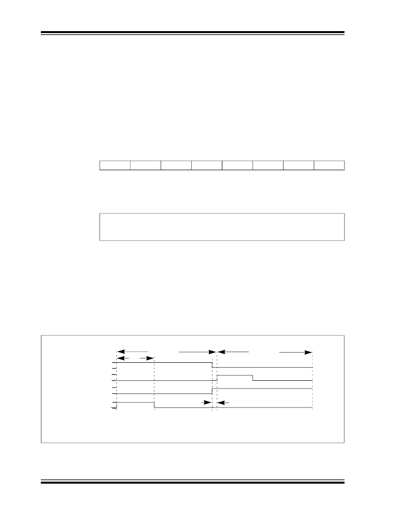
FIGURE 8-10: PWM DIRECTION CHANGE
R/W-0
P1DEL7
bit 7
R/W-0
P1DEL6
R/W-0
P1DEL5
R/W-0
P1DEL4
R/W-0
P1DEL3
R/W-0
P1DEL2
R/W-0
P1DEL1
R/W-0
P1DEL0
bit 0
bit 7-0
P1DEL<7:0>: PWM Delay Count for Half-Bridge Output Mode:
Number of F
OSC
/4 (Tosc
4)
cycles between the P1A transition and the P1B transition.
Legend:
R = Readable bit
- n = Value at POR
W = Writable bit
’
1
’
= Bit is set
U = Unimplemented bit, read as
‘
0
’
’
0
’
= Bit is cleared
x = Bit is unknown
DC
PERIOD
SIGNAL
P1A (Active High)
Note 1:
The Direction bit in the ECCP Control Register (CCP1CON<PWM1M1>) is written anytime during the PWM cycle.
The P1A and P1C signals switch T
OSC
, 4*Tosc or 16*T
OSC
, depending on the Timer2 prescaler value, earlier when
changing direction. The modulated P1B and P1D signals are inactive at this time.
2:
(1)
PERIOD
(2)
P1D (Active High)
P1C (Active High)
P1B (Active High)
相關(guān)PDF資料 |
PDF描述 |
|---|---|
| PIC16C770 | 8-Bit CMOS Microcontrollers(8位CMOS微控制器) |
| PIC16C771 | 8-Bit CMOS Microcontrollers(8位CMOS微控制器) |
| PIC16C73A | 8-Bit CMOS Microcontrollers with A/D Converter |
| PIC16C76 | 8-Bit CMOS Microcontrollers with A/D Converter(每個I/O口有25mA驅(qū)動/吸收電流,并行從動口,2路捕捉/比較/PWM的微控制器) |
| PIC16C77 | 8-Bit CMOS Microcontrollers with A/D Converter(每個I/O口有25mA驅(qū)動/吸收電流,并行從動口,1路捕捉/比較/PWM的微控制器) |
相關(guān)代理商/技術(shù)參數(shù) |
參數(shù)描述 |
|---|---|
| PIC16C717/JW | 功能描述:8位微控制器 -MCU 3.5KB 256 RAM 16 I/O RoHS:否 制造商:Silicon Labs 核心:8051 處理器系列:C8051F39x 數(shù)據(jù)總線寬度:8 bit 最大時鐘頻率:50 MHz 程序存儲器大小:16 KB 數(shù)據(jù) RAM 大小:1 KB 片上 ADC:Yes 工作電源電壓:1.8 V to 3.6 V 工作溫度范圍:- 40 C to + 105 C 封裝 / 箱體:QFN-20 安裝風格:SMD/SMT |
| PIC16C717/P | 功能描述:8位微控制器 -MCU 3.5KB 256 RAM 16 I/O RoHS:否 制造商:Silicon Labs 核心:8051 處理器系列:C8051F39x 數(shù)據(jù)總線寬度:8 bit 最大時鐘頻率:50 MHz 程序存儲器大小:16 KB 數(shù)據(jù) RAM 大小:1 KB 片上 ADC:Yes 工作電源電壓:1.8 V to 3.6 V 工作溫度范圍:- 40 C to + 105 C 封裝 / 箱體:QFN-20 安裝風格:SMD/SMT |
| PIC16C717/P | 制造商:Microchip Technology Inc 功能描述:IC 8BIT CMOS MCU 16C717 DIP18 |
| PIC16C717/P | 制造商:Microchip Technology Inc 功能描述:Microcontroller IC Number of I/Os:16 |
| PIC16C717/PC01 | 制造商:Microchip Technology Inc 功能描述: |
發(fā)布緊急采購,3分鐘左右您將得到回復。