- 您現(xiàn)在的位置:買賣IC網(wǎng) > PDF目錄368024 > PIC16C717 (Microchip Technology Inc.) 8-Bit CMOS Microcontrollers(8位CMOS微控制器) PDF資料下載
參數(shù)資料
| 型號: | PIC16C717 |
| 廠商: | Microchip Technology Inc. |
| 英文描述: | 8-Bit CMOS Microcontrollers(8位CMOS微控制器) |
| 中文描述: | 8位CMOS微控制器(8位的CMOS微控制器) |
| 文件頁數(shù): | 59/220頁 |
| 文件大小: | 3585K |
| 代理商: | PIC16C717 |
第1頁第2頁第3頁第4頁第5頁第6頁第7頁第8頁第9頁第10頁第11頁第12頁第13頁第14頁第15頁第16頁第17頁第18頁第19頁第20頁第21頁第22頁第23頁第24頁第25頁第26頁第27頁第28頁第29頁第30頁第31頁第32頁第33頁第34頁第35頁第36頁第37頁第38頁第39頁第40頁第41頁第42頁第43頁第44頁第45頁第46頁第47頁第48頁第49頁第50頁第51頁第52頁第53頁第54頁第55頁第56頁第57頁第58頁當(dāng)前第59頁第60頁第61頁第62頁第63頁第64頁第65頁第66頁第67頁第68頁第69頁第70頁第71頁第72頁第73頁第74頁第75頁第76頁第77頁第78頁第79頁第80頁第81頁第82頁第83頁第84頁第85頁第86頁第87頁第88頁第89頁第90頁第91頁第92頁第93頁第94頁第95頁第96頁第97頁第98頁第99頁第100頁第101頁第102頁第103頁第104頁第105頁第106頁第107頁第108頁第109頁第110頁第111頁第112頁第113頁第114頁第115頁第116頁第117頁第118頁第119頁第120頁第121頁第122頁第123頁第124頁第125頁第126頁第127頁第128頁第129頁第130頁第131頁第132頁第133頁第134頁第135頁第136頁第137頁第138頁第139頁第140頁第141頁第142頁第143頁第144頁第145頁第146頁第147頁第148頁第149頁第150頁第151頁第152頁第153頁第154頁第155頁第156頁第157頁第158頁第159頁第160頁第161頁第162頁第163頁第164頁第165頁第166頁第167頁第168頁第169頁第170頁第171頁第172頁第173頁第174頁第175頁第176頁第177頁第178頁第179頁第180頁第181頁第182頁第183頁第184頁第185頁第186頁第187頁第188頁第189頁第190頁第191頁第192頁第193頁第194頁第195頁第196頁第197頁第198頁第199頁第200頁第201頁第202頁第203頁第204頁第205頁第206頁第207頁第208頁第209頁第210頁第211頁第212頁第213頁第214頁第215頁第216頁第217頁第218頁第219頁第220頁
2002 Microchip Technology Inc.
DS41120B-page 57
PIC16C717/770/771
8.3.2
PWM DUTY CYCLE
The PWM duty cycle is specified by writing to the
CCPR1L register and to the CCP1CON<5:4> bits. Up
to 10-bit resolution is available. The CCPR1L contains
the eight MSbs and the CCP1CON<5:4> contains the
two LSbs. This 10-bit value is represented by
CCPR1L:CCP1CON<5:4>. The following equation is
used to calculate the PWM duty cycle in time:
PWM duty cycle = (CCPR1L:CCP1CON<5:4>)
T
OSC
(TMR2 prescale value)
CCPR1L and CCP1CON<5:4> can be written to at any
time, but the duty cycle value is not latched into
CCPR1H until after a match between PR2 and TMR2
occurs (i.e., the period is complete). In PWM mode,
CCPR1H is a read-only register.
The CCPR1H register and a 2-bit internal latch are
used to double buffer the PWM duty cycle. This double
buffering is essential for glitchless PWM operation.
When the CCPR1H and 2-bit latch match TMR2 con-
catenated with an internal 2-bit Q clock or 2 bits of the
TMR2 prescaler, the CCP1 pin is cleared.
Maximum PWM resolution (bits) for a given PWM fre-
quency:
8.3.3
PWM OUTPUT CONFIGURATIONS
The PWM1M1 bits in the CCP1CON register allows
one of the following configurations:
Single output
Half-Bridge output
Full-Bridge output, Forward mode
Full-Bridge output, Reverse mode
In the Single Output mode, the RB3/CCP1/P1A pin is
used as the PWM output. Since the CCP1 output is
multiplexed with the PORTB<3> data latch, the
TRISB<3> bit must be cleared to make the CCP1 pin
an output.
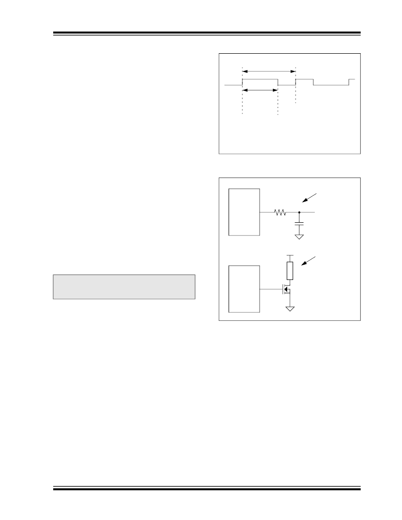
FIGURE 8-4:
SINGLE PWM OUTPUT
FIGURE 8-5:
EXAMPLE OF SINGLE
OUTPUT APPLICATION
In the Half-Bridge Output mode, two pins are used as
outputs. The RB3/CCP1/P1A pin has the PWM output
signal, while the RB5/SDO/P1B pin has the comple-
mentary PWM output signal. This mode can be used
for half-bridge applications, as shown on Figure 8-7, or
for full-bridge applications, where four power switches
are being modulated with two PWM signal.
Since the P1A and P1B outputs are multiplexed with
the PORTB<3> and PORTB<5> data latches, the
TRISB<3> and TRISB<5> bits must be cleared to con-
figure P1A and P1B as outputs.
In Half-Bridge Output mode, the programmable dead-
band delay can be used to prevent shoot-through cur-
rent in bridge power devices. See Section 8.3.5 for
more details of the deadband delay operations.
Note:
If the PWM duty cycle value is longer than
the PWM period, the CCP1 pin will not be
cleared.
OSC
F
2
log
-F
log
-----------------------------bits
=
Period
Duty Cycle
(1)
(1)
Note 1:
At this time, the TMR2 register is equal to the PR2 register.
2:
Output signal is shown as asserted high.
CCP1
(2)
C
PIC16C717/770/771
CCP1
R
Vout
Using PWM as
a D/A Converter
PIC16C717/770/771
CCP1
Using PWM to
Drive a Power
Load
V+
L
O
A
D
相關(guān)PDF資料 |
PDF描述 |
|---|---|
| PIC16C770 | 8-Bit CMOS Microcontrollers(8位CMOS微控制器) |
| PIC16C771 | 8-Bit CMOS Microcontrollers(8位CMOS微控制器) |
| PIC16C73A | 8-Bit CMOS Microcontrollers with A/D Converter |
| PIC16C76 | 8-Bit CMOS Microcontrollers with A/D Converter(每個I/O口有25mA驅(qū)動/吸收電流,并行從動口,2路捕捉/比較/PWM的微控制器) |
| PIC16C77 | 8-Bit CMOS Microcontrollers with A/D Converter(每個I/O口有25mA驅(qū)動/吸收電流,并行從動口,1路捕捉/比較/PWM的微控制器) |
相關(guān)代理商/技術(shù)參數(shù) |
參數(shù)描述 |
|---|---|
| PIC16C717/JW | 功能描述:8位微控制器 -MCU 3.5KB 256 RAM 16 I/O RoHS:否 制造商:Silicon Labs 核心:8051 處理器系列:C8051F39x 數(shù)據(jù)總線寬度:8 bit 最大時鐘頻率:50 MHz 程序存儲器大小:16 KB 數(shù)據(jù) RAM 大小:1 KB 片上 ADC:Yes 工作電源電壓:1.8 V to 3.6 V 工作溫度范圍:- 40 C to + 105 C 封裝 / 箱體:QFN-20 安裝風(fēng)格:SMD/SMT |
| PIC16C717/P | 功能描述:8位微控制器 -MCU 3.5KB 256 RAM 16 I/O RoHS:否 制造商:Silicon Labs 核心:8051 處理器系列:C8051F39x 數(shù)據(jù)總線寬度:8 bit 最大時鐘頻率:50 MHz 程序存儲器大小:16 KB 數(shù)據(jù) RAM 大小:1 KB 片上 ADC:Yes 工作電源電壓:1.8 V to 3.6 V 工作溫度范圍:- 40 C to + 105 C 封裝 / 箱體:QFN-20 安裝風(fēng)格:SMD/SMT |
| PIC16C717/P | 制造商:Microchip Technology Inc 功能描述:IC 8BIT CMOS MCU 16C717 DIP18 |
| PIC16C717/P | 制造商:Microchip Technology Inc 功能描述:Microcontroller IC Number of I/Os:16 |
| PIC16C717/PC01 | 制造商:Microchip Technology Inc 功能描述: |
發(fā)布緊急采購,3分鐘左右您將得到回復(fù)。