- 您現(xiàn)在的位置:買(mǎi)賣IC網(wǎng) > PDF目錄367934 > PH28F640L18T85 (INTEL CORP) StrataFlash Wireless Memory PDF資料下載
參數(shù)資料
| 型號(hào): | PH28F640L18T85 |
| 廠商: | INTEL CORP |
| 元件分類: | PROM |
| 英文描述: | StrataFlash Wireless Memory |
| 中文描述: | 4M X 16 FLASH 1.8V PROM, 85 ns, PBGA56 |
| 封裝: | 0.75 MM PITCH, LEAD FREE, VFBGA-56 |
| 文件頁(yè)數(shù): | 51/106頁(yè) |
| 文件大小: | 1272K |
| 代理商: | PH28F640L18T85 |
第1頁(yè)第2頁(yè)第3頁(yè)第4頁(yè)第5頁(yè)第6頁(yè)第7頁(yè)第8頁(yè)第9頁(yè)第10頁(yè)第11頁(yè)第12頁(yè)第13頁(yè)第14頁(yè)第15頁(yè)第16頁(yè)第17頁(yè)第18頁(yè)第19頁(yè)第20頁(yè)第21頁(yè)第22頁(yè)第23頁(yè)第24頁(yè)第25頁(yè)第26頁(yè)第27頁(yè)第28頁(yè)第29頁(yè)第30頁(yè)第31頁(yè)第32頁(yè)第33頁(yè)第34頁(yè)第35頁(yè)第36頁(yè)第37頁(yè)第38頁(yè)第39頁(yè)第40頁(yè)第41頁(yè)第42頁(yè)第43頁(yè)第44頁(yè)第45頁(yè)第46頁(yè)第47頁(yè)第48頁(yè)第49頁(yè)第50頁(yè)當(dāng)前第51頁(yè)第52頁(yè)第53頁(yè)第54頁(yè)第55頁(yè)第56頁(yè)第57頁(yè)第58頁(yè)第59頁(yè)第60頁(yè)第61頁(yè)第62頁(yè)第63頁(yè)第64頁(yè)第65頁(yè)第66頁(yè)第67頁(yè)第68頁(yè)第69頁(yè)第70頁(yè)第71頁(yè)第72頁(yè)第73頁(yè)第74頁(yè)第75頁(yè)第76頁(yè)第77頁(yè)第78頁(yè)第79頁(yè)第80頁(yè)第81頁(yè)第82頁(yè)第83頁(yè)第84頁(yè)第85頁(yè)第86頁(yè)第87頁(yè)第88頁(yè)第89頁(yè)第90頁(yè)第91頁(yè)第92頁(yè)第93頁(yè)第94頁(yè)第95頁(yè)第96頁(yè)第97頁(yè)第98頁(yè)第99頁(yè)第100頁(yè)第101頁(yè)第102頁(yè)第103頁(yè)第104頁(yè)第105頁(yè)第106頁(yè)
Intel StrataFlash Wireless Memory (L18)
Datasheet
Intel StrataFlash Wireless Memory (L18)
Order Number: 251902, Revision: 009
April 2005
51
During synchronous array and non-array read modes, the first word is output from the data buffer
on the next valid CLK edge after the initial access latency delay (see
Section 10.3.2, “Latency
Count” on page 52
). Subsequent data is output on valid CLK edges following a minimum delay.
However, for a synchronous non-array read, the same word of data will be output on successive
clock edges until the burst length requirements are satisfied.
Figure 14Figure 16
10.2.1
Burst Suspend
The Burst Suspend feature of the device can reduce or eliminate the initial access latency incurred
when system software needs to suspend a burst sequence that is in progress in order to retrieve data
from another device on the same system bus. The system processor can resume the burst sequence
later. Burst suspend provides maximum benefit in non-cache systems.
Burst accesses can be suspended during the initial access latency (before data is received) or after
the device has output data. When a burst access is suspended, internal array sensing continues and
any previously latched internal data is retained. A burst sequence can be suspended and resumed
without limit as long as device operation conditions are met.
Burst Suspend occurs when CE# is asserted, the current address has been latched (either ADV#
rising edge or valid CLK edge), CLK is halted, and OE# is deasserted. CLK can be halted when it
is at V
IH
or V
IL
. WAIT is in High-Z during OE# deassertion.
To resume the burst access, OE# is reasserted, and CLK is restarted. Subsequent CLK edges
resume the burst sequence.
Within the device, CE# and OE# gate WAIT. Therefore, during Burst Suspend WAIT is placed in
high-impedance state when OE# is deasserted and resumed active when OE# is re-asserted. See
Figure 17, “Burst Suspend Timing” on page 36
.
10.3
Read Configuration Register (RCR)
The RCR is used to select the read mode (synchronous or asynchronous), and it defines the
synchronous burst characteristics of the device. To modify RCR settings, use the Configure Read
Configuration Register command (see
Section 9.2, “Device Commands” on page 47
).
RCR contents can be examined using the Read Device Identifier command, and then reading from
<partition base address> + 0x05 (see
Section 15.2, “Read Device Identifier” on page 76
).
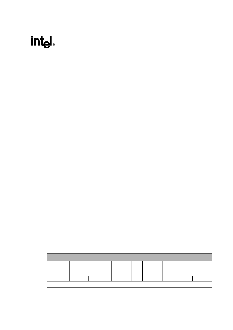
The RCR is shown in
Table 10
. The following sections describe each RCR bit.
Table 10.
Read Configuration Register Description (Sheet 1 of 2)
Read Configuration Register (RCR)
Read
Mode
RES
Latency Count
WAIT
Polarity
Data
Hold
WAIT
Delay
Burst
Seq
CLK
Edge
RES
RES
Burst
Wrap
Burst Length
RM
R
LC[2:0]
WP
DH
WD
BS
CE
R
R
BW
BL[2:0]
15
14
13
12
11
10
9
8
7
6
5
4
3
2
1
0
Bit
Name
Description
相關(guān)PDF資料 |
PDF描述 |
|---|---|
| PH2907A | PNP switching transistor |
| PH2907 | PNP switching transistor |
| PH2931-135S | Rail-to-Rail, Very Low Noise Universal Dual Filter Building Block; Package: SO; No of Pins: 16; Temperature Range: -40°C to +85°C |
| PH2931-I3 | Radar Pulsed Power Transistor, 135W, 20ms Pulse, 1% Duty 2.9 - 3.1 GHz |
| PH2931-20M | Radar Pulsed Power Transistor, 20W,100ms Pulse, 10% Duty 2.9-3.1 GHz |
相關(guān)代理商/技術(shù)參數(shù) |
參數(shù)描述 |
|---|---|
| PH28F640W18BD60 | 制造商:Micron Technology Inc 功能描述:PH28F640W18BD60S L785 |
| PH28F640W18BD60B | 制造商:Micron Technology Inc 功能描述:NUMPH28F640W18BD60B PH28F640W18BD60S L78 |
| PH28F640W18TE60B | 制造商:Micron Technology Inc 功能描述:64MB, CRYSTAL .75 VFBGA 1.8 LF - Tape and Reel |
| PH28F640W30BD70A | 制造商:Micron Technology Inc 功能描述:NOR Flash Parallel/Serial 1.8V 64Mbit 4M x 16bit 70ns 56-Pin VFBGA Tray 制造商:Micron Technology Inc 功能描述:NUMPH28F640W30BD70A MM#862859FLASH 28F64 |
| PH2-8-SGA | 制造商:Adam Technologies Inc 功能描述:PH2 Series Dual Row 8 Position Straight 2.54 mm Centerline Pin Header |
發(fā)布緊急采購(gòu),3分鐘左右您將得到回復(fù)。