- 您現(xiàn)在的位置:買賣IC網(wǎng) > PDF目錄378045 > PCI1510GVF (Texas Instruments, Inc.) PC CARD CONTROLLERS PDF資料下載
參數(shù)資料
| 型號: | PCI1510GVF |
| 廠商: | Texas Instruments, Inc. |
| 英文描述: | PC CARD CONTROLLERS |
| 中文描述: | PC卡控制器 |
| 文件頁數(shù): | 54/128頁 |
| 文件大小: | 735K |
| 代理商: | PCI1510GVF |
第1頁第2頁第3頁第4頁第5頁第6頁第7頁第8頁第9頁第10頁第11頁第12頁第13頁第14頁第15頁第16頁第17頁第18頁第19頁第20頁第21頁第22頁第23頁第24頁第25頁第26頁第27頁第28頁第29頁第30頁第31頁第32頁第33頁第34頁第35頁第36頁第37頁第38頁第39頁第40頁第41頁第42頁第43頁第44頁第45頁第46頁第47頁第48頁第49頁第50頁第51頁第52頁第53頁當(dāng)前第54頁第55頁第56頁第57頁第58頁第59頁第60頁第61頁第62頁第63頁第64頁第65頁第66頁第67頁第68頁第69頁第70頁第71頁第72頁第73頁第74頁第75頁第76頁第77頁第78頁第79頁第80頁第81頁第82頁第83頁第84頁第85頁第86頁第87頁第88頁第89頁第90頁第91頁第92頁第93頁第94頁第95頁第96頁第97頁第98頁第99頁第100頁第101頁第102頁第103頁第104頁第105頁第106頁第107頁第108頁第109頁第110頁第111頁第112頁第113頁第114頁第115頁第116頁第117頁第118頁第119頁第120頁第121頁第122頁第123頁第124頁第125頁第126頁第127頁第128頁
316
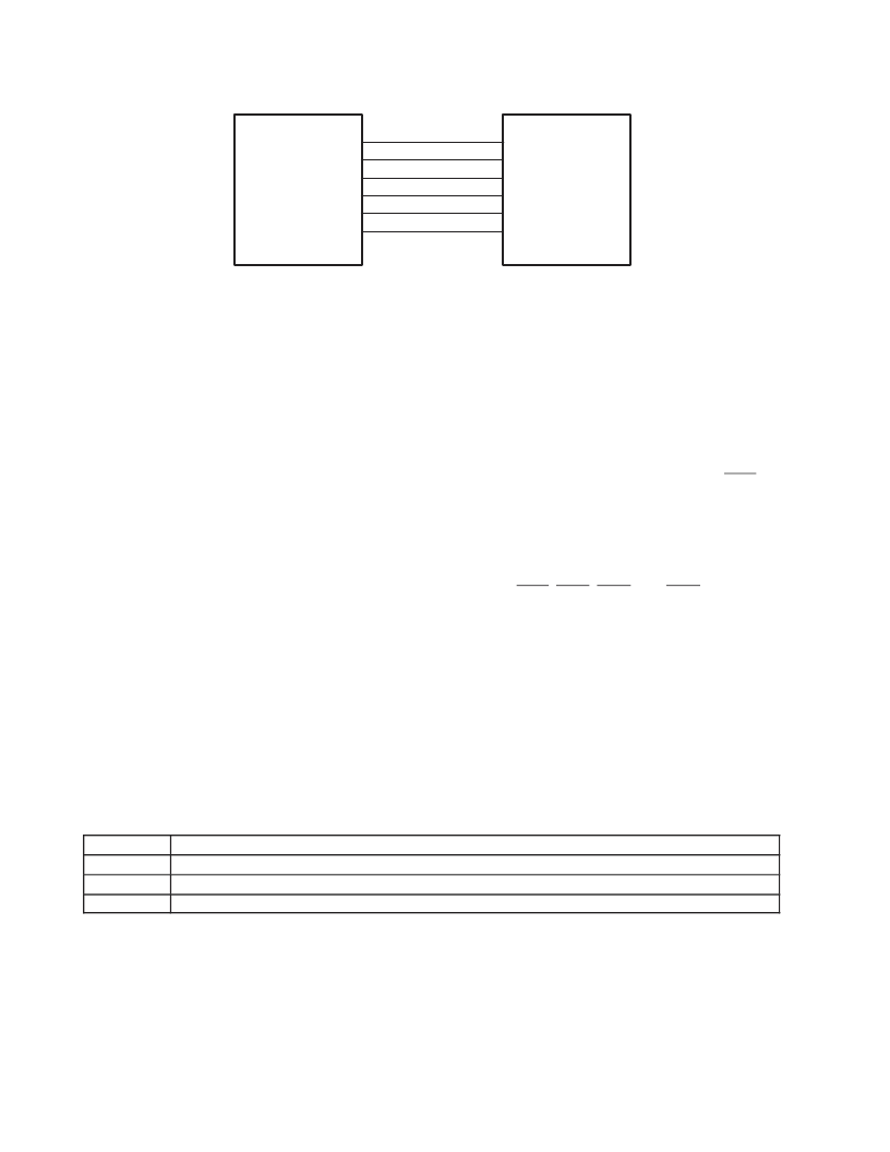
PCI1510
PIC
MFUNC1
MFUNC2
MFUNC3
MFUNC4
MFUNC5
MFUNC6
IRQ3
IRQ4
IRQ5
IRQ10
IRQ11
IRQ15
Figure 314. IRQ Implementation
Power-on software is responsible for programming the multifunction routing register to reflect the IRQ configuration
of a system implementing the controller. See Section 4.30,
Multifunction Routing Register
,
for details on configuring
the multifunction terminals.
The parallel ISA-type IRQ signaling from the MFUNC6MFUNC0 terminals is compatible with the input signal
requirements of the 8259 PIC. The parallel IRQ option is provided for system designs that require legacy ISA IRQs.
Design constraints may demand more MFUNC6MFUNC0 IRQ terminals than the controller makes available.
3.7.4
Using Parallel PCI Interrupts
Parallel PCI interrupts are available when exclusively in parallel PCI interrupt/parallel ISA IRQ signaling mode, and
when only IRQs are serialized with the IRQSER protocol. Socket functional interrupts can be routed to INTA.
3.7.5
Using Serialized IRQSER Interrupts
The serialized interrupt protocol implemented in the controller uses a single terminal to communicate all interrupt
status information to the host controller. The protocol defines a serial packet consisting of a start cycle, multiple
interrupt indication cycles, and a stop cycle. All data in the packet is synchronous with the PCI clock. The packet data
describes 16 parallel ISA IRQ signals and the optional 4 PCI interrupts INTA, INTB, INTC, and INTD. For details on
the IRQSER protocol, refer to the document
Serialized IRQ Support for PCI Systems
.
3.7.6
SMI Support in the PCI1510 Controller
The controller provides a mechanism for interrupting the system when power changes have been made to the PC
Card socket interfaces. The interrupt mechanism is designed to fit into a system maintenance interrupt (SMI) scheme.
SMI interrupts are generated by the controller, when enabled, after a write cycle to either the socket control register
(CB offset 10h, see Section 6.5) of the CardBus register set, or the ExCA power control register (ExCA offset
02h/42h/802h, see Section 5.3) causes a power cycle change sequence to be sent on the power switch interface.
The SMI control is programmed through three bits in the system control register (PCI offset 80h, see Section 4.29).
These bits are SMIROUTE (bit 26), SMISTATUS (bit 25), and SMIENB (bit 24). Table 39 describes the SMI control
bits function.
Table 39. SMI Control
BIT NAME
FUNCTION
SMIROUTE
This shared bit controls whether the SMI interrupts are sent as a CSC interrupt or as IRQ2.
SMISTAT
This socket dependent bit is set when an SMI interrupt is pending. This status flag is cleared by writing back 1b.
SMIENB
When set, SMI interrupt generation is enabled.
If CSC SMI interrupts are selected, then the SMI interrupt is sent as the CSC on a per-socket basis. The CSC interrupt
can be either level or edge mode, depending upon the CSCMODE bit in the ExCA global control register (ExCA offset
1Eh/5Eh/81Eh, see Section 5.20).
If IRQ2 is selected by SMIROUTE, then the IRQSER signaling protocol supports SMI signaling in the IRQ2 IRQ/Data
slot. In a parallel ISA IRQ system, the support for an active low IRQ2 is provided only if IRQ2 is routed to either
MFUNC3 or MFUNC6 through the multifunction routing register (PCI offset 8Ch, see Section 4.30).
相關(guān)PDF資料 |
PDF描述 |
|---|---|
| PCI1510ZVF | PC CARD CONTROLLERS |
| PCI1520I | PC CARD CONTROLLERS |
| PCI4410A | PC CARD AND OHCI CONTROLLER |
| PCI4510PDV | PC CARD AND INTEGRATED 1394A-2000 OHCI TWO PORT PHY/LINK LAYER CONTROLLER |
| PCI4515 | SINGLE SOCKET CARDBUS CONTROLLER WITH INTEGRATED |
相關(guān)代理商/技術(shù)參數(shù) |
參數(shù)描述 |
|---|---|
| PCI1510PGE | 功能描述:外圍驅(qū)動器與原件 - PCI Single Slot PC CardBus Controller RoHS:否 制造商:PLX Technology 工作電源電壓: 最大工作溫度: 安裝風(fēng)格:SMD/SMT 封裝 / 箱體:FCBGA-1156 封裝:Tray |
| PCI1510PGEG4 | 功能描述:外圍驅(qū)動器與原件 - PCI Single Slot PC CardBus Controller RoHS:否 制造商:PLX Technology 工作電源電壓: 最大工作溫度: 安裝風(fēng)格:SMD/SMT 封裝 / 箱體:FCBGA-1156 封裝:Tray |
| PCI1510RGVF | 功能描述:IC PC CARD CONTROLLER 253-BGA RoHS:是 類別:集成電路 (IC) >> 接口 - 控制器 系列:- 標(biāo)準(zhǔn)包裝:4,900 系列:- 控制器類型:USB 2.0 控制器 接口:串行 電源電壓:3 V ~ 3.6 V 電流 - 電源:135mA 工作溫度:0°C ~ 70°C 安裝類型:表面貼裝 封裝/外殼:36-VFQFN 裸露焊盤 供應(yīng)商設(shè)備封裝:36-QFN(6x6) 包裝:* 其它名稱:Q6396337A |
| PCI1510RZVF | 功能描述:外圍驅(qū)動器與原件 - PCI PC CARD CONTROLLERS RoHS:否 制造商:PLX Technology 工作電源電壓: 最大工作溫度: 安裝風(fēng)格:SMD/SMT 封裝 / 箱體:FCBGA-1156 封裝:Tray |
| PCI1510ZGU | 功能描述:外圍驅(qū)動器與原件 - PCI Single Slot PC CardBus Controller RoHS:否 制造商:PLX Technology 工作電源電壓: 最大工作溫度: 安裝風(fēng)格:SMD/SMT 封裝 / 箱體:FCBGA-1156 封裝:Tray |
發(fā)布緊急采購,3分鐘左右您將得到回復(fù)。