- 您現(xiàn)在的位置:買賣IC網(wǎng) > PDF目錄367816 > PCF2113F2 (NXP Semiconductors N.V.) LCD controller/driver(LCD控制器/驅(qū)動(dòng)器) PDF資料下載
參數(shù)資料
| 型號(hào): | PCF2113F2 |
| 廠商: | NXP Semiconductors N.V. |
| 英文描述: | LCD controller/driver(LCD控制器/驅(qū)動(dòng)器) |
| 中文描述: | LCD控制器/驅(qū)動(dòng)器(液晶顯示控制器/驅(qū)動(dòng)器) |
| 文件頁數(shù): | 7/60頁 |
| 文件大小: | 392K |
| 代理商: | PCF2113F2 |
第1頁第2頁第3頁第4頁第5頁第6頁當(dāng)前第7頁第8頁第9頁第10頁第11頁第12頁第13頁第14頁第15頁第16頁第17頁第18頁第19頁第20頁第21頁第22頁第23頁第24頁第25頁第26頁第27頁第28頁第29頁第30頁第31頁第32頁第33頁第34頁第35頁第36頁第37頁第38頁第39頁第40頁第41頁第42頁第43頁第44頁第45頁第46頁第47頁第48頁第49頁第50頁第51頁第52頁第53頁第54頁第55頁第56頁第57頁第58頁第59頁第60頁
1997 Apr 04
7
Philips Semiconductors
Product specification
LCD controller/driver
PCF2113x
7
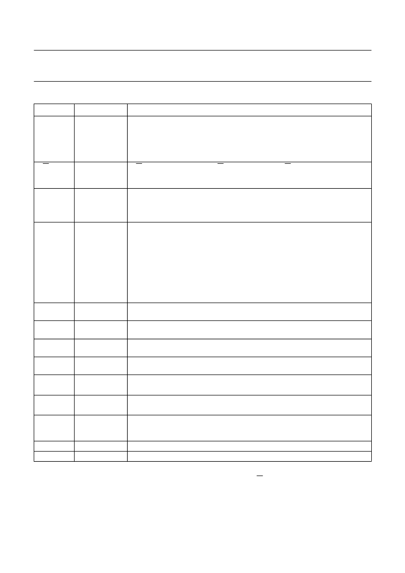
PIN FUNCTIONS
Note
1.
If the 4-bit interface is used without reading out from the PCF2113x (i.e. R/W is set permanently to logic 0), the
unused ports DB0 to DB3 can either be set to V
SS
or V
DD
instead of leaving them open.
NAME
FUNCTION
DESCRIPTION
RS
register select
RS selects the register to be accessed for read and write when the device is
controlled by the parallel interface. There is an internal pull-up on this pin.
RS = logic 0 selects the instruction register for write and the Busy Flag and Address
Counter for read.
RS = logic 1 selects the data register for both read and write.
R/W selects either the read (R/W = logic 1) or write (R/W = logic 0) operation when
the device is controlled by the parallel interface. There is an internal pull-up on this
pin.
The E pin is set HIGH to signal the start of a read or write operation when the device
is controlled by the parallel interface. Data is clocked in or out of the chip on the
negative edge of the clock. Note that this pin must be tied to logic 0 (V
SS
) when
I
2
C-bus control is used.
The parallel interface of the device. This bi-directional, 3-state data bus transfers
data between the system controller and the PCF2113x. There is an internal pull-up
on each of the data lines.
DB7 to DB0 must be connected to V
DD
or left open circuit when I
2
C-bus control is
used. Note that DB3 shares the same pin as SA0.
In 4-bit operations only DB7 to DB4 are used, and DB3 to DB0 must be left open
circuit. See note 1.
DB7 may be used as the Busy Flag, signalling that internal operations are not yet
completed.
These pins output the data for columns.
R/W
read/write
E
data bus clock
DB7 to DB0
data bus
C1 to C60
column driver
outputs
row driver
outputs
LCD power
supply
oscillator
R1 to R18
These pins output the row select waveforms to the display.
R17 and R18 drive the icons.
Positive power supply for the liquid crystal display. This may be generated on-chip or
supplied externally.
When the on-chip oscillator is used this pin must be connected to V
DD
.
An external clock signal, if used, is input at this pin.
Input for the I
2
C-bus clock signal.
SCL must be connected to V
SS
or V
DD
when the parallel interface is used.
I/O for the I
2
C-bus data line.
SDA must be connected to V
SS
or V
DD
when the parallel interface is used.
The hardware sub-address line is used to program the device sub-address for two
different PCF2113xs on the same I
2
C bus. Note that SA0 shares the same pin as
DB3.
T1 must be connected to V
SS
and is not user accessible.
power-down pad PD selects chip power-down mode. For normal operation PD = logic 0.
V
LCD
OSC
SCL
serial clock line
SDA
serial data line
SA0
address pin
T1
PD
test pad
相關(guān)PDF資料 |
PDF描述 |
|---|---|
| PCF211310 | LCD controller/driver(LCD控制器/驅(qū)動(dòng)器) |
| PCF21132 | LCD controller/driver(LCD控制器/驅(qū)動(dòng)器) |
| PCF211410 | LCD controller/drivers(LCD控制器/驅(qū)動(dòng)器) |
| PCF2116AHZ | JT 66C 66#22D PIN RECP |
| PCF2116CHZ | LCD controller/drivers |
相關(guān)代理商/技術(shù)參數(shù) |
參數(shù)描述 |
|---|---|
| PCF2113FAMILY | 制造商:未知廠家 制造商全稱:未知廠家 功能描述:LCD Display Driver |
| PCF2113WU | 制造商:PHILIPS 制造商全稱:NXP Semiconductors 功能描述:LCD controllers/drivers |
| PCF2113WU/2/F4 | 制造商:PHILIPS 制造商全稱:NXP Semiconductors 功能描述:LCD controllers/drivers |
| PCF2113WU/2/F4,026 | 功能描述:IC LCD CTLR/DRIVER UNCASED RoHS:是 類別:未定義的類別 >> 其它 系列:* 標(biāo)準(zhǔn)包裝:1 系列:* 其它名稱:MS305720A |
| PCF2113WU2 | 制造商:PHILIPS 制造商全稱:NXP Semiconductors 功能描述:LCD controllers/drivers |
發(fā)布緊急采購(gòu),3分鐘左右您將得到回復(fù)。