- 您現(xiàn)在的位置:買賣IC網(wǎng) > PDF目錄11733 > ORSO42G5-3BMN484C (Lattice Semiconductor Corporation)IC TRANCEIVERS FPSC 680FPGAM PDF資料下載
參數(shù)資料
| 型號: | ORSO42G5-3BMN484C |
| 廠商: | Lattice Semiconductor Corporation |
| 文件頁數(shù): | 81/153頁 |
| 文件大小: | 0K |
| 描述: | IC TRANCEIVERS FPSC 680FPGAM |
| 產(chǎn)品變化通告: | Product Discontinuation 01/Aug/2011 |
| 標準包裝: | 60 |
| 系列: | * |
第1頁第2頁第3頁第4頁第5頁第6頁第7頁第8頁第9頁第10頁第11頁第12頁第13頁第14頁第15頁第16頁第17頁第18頁第19頁第20頁第21頁第22頁第23頁第24頁第25頁第26頁第27頁第28頁第29頁第30頁第31頁第32頁第33頁第34頁第35頁第36頁第37頁第38頁第39頁第40頁第41頁第42頁第43頁第44頁第45頁第46頁第47頁第48頁第49頁第50頁第51頁第52頁第53頁第54頁第55頁第56頁第57頁第58頁第59頁第60頁第61頁第62頁第63頁第64頁第65頁第66頁第67頁第68頁第69頁第70頁第71頁第72頁第73頁第74頁第75頁第76頁第77頁第78頁第79頁第80頁當前第81頁第82頁第83頁第84頁第85頁第86頁第87頁第88頁第89頁第90頁第91頁第92頁第93頁第94頁第95頁第96頁第97頁第98頁第99頁第100頁第101頁第102頁第103頁第104頁第105頁第106頁第107頁第108頁第109頁第110頁第111頁第112頁第113頁第114頁第115頁第116頁第117頁第118頁第119頁第120頁第121頁第122頁第123頁第124頁第125頁第126頁第127頁第128頁第129頁第130頁第131頁第132頁第133頁第134頁第135頁第136頁第137頁第138頁第139頁第140頁第141頁第142頁第143頁第144頁第145頁第146頁第147頁第148頁第149頁第150頁第151頁第152頁第153頁
Lattice Semiconductor
ORCA ORSO42G5 and ORSO82G5 Data Sheet
33
tee that this elastic store will not be overrun. The 32:8 MUX is also responsible for producing the divide-by-4 clock
from the SERDES output clock (XCK311) which is 311.04 MHz at a line rate of 2.488 Gbps.
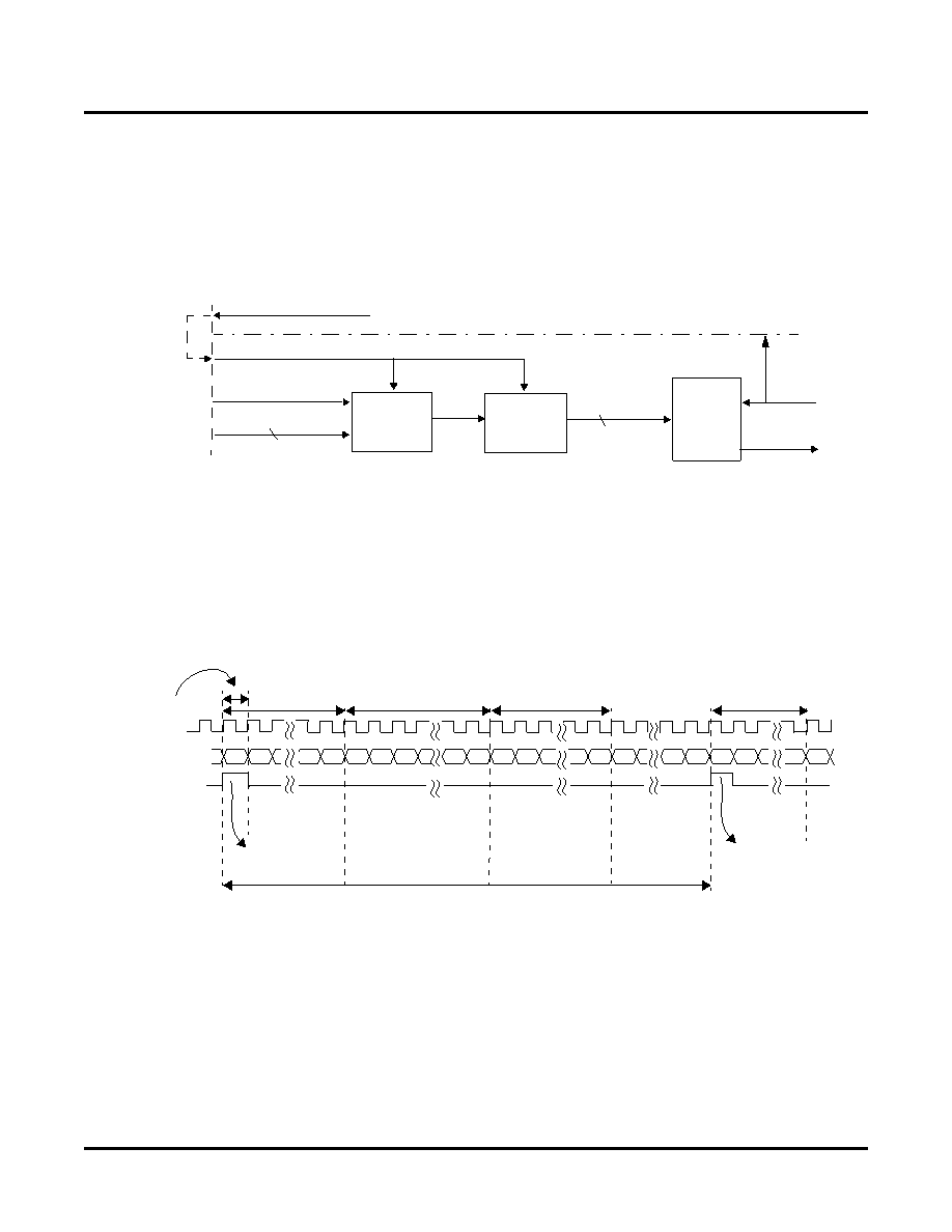
SONET Mode Transmit Timing
Figure 17 shows the transmit clocks and a recommended clocking scheme. As shown, TCK78[A,B] can be used to
the source TSYSCLKxx signals. It is a requirement that TSYSCLKxx be frequency locked to the corresponding
TCK78[A,B] clock signal derived from REFCLK_[A:B].
Figure 17. Transmit Clocking Diagram in SONET Mode
When operating in SONET mode, the entire SONET frame is sent by the user. Optionally the TOH bytes can be
overwritten by the transmit block (AUTO_SOH or AUTO_TOH) before sending to scrambler and SERDES block.
Each SONET frame is 125 s given a 155.52MHz reference clock.
The frame starts with 36 clock cycles (77.76 MHz) of TOH followed by 1044 clock cycles of SPE, followed by
36 clock cycles of TOH, 1044 cycles of SPE etc. for all nine rows.
Figure 18. Transmit SONET Mode
SONET Mode Receive Path
The receiver block receives a byte from the SERDES blocks for each of the channels. The byte arrives at the
receiver block at 311.04 MHz. This data are not frame-aligned or word aligned. The data are rst passed through a
divide-by-4 DEMUX which produces a 32-bit word at 77.76 MHz. Data from the DEMUX is then passed through a
framer which aligns and frames the data. Data are processed based on cell mode or SONET mode.
In the SONET mode, the descrambled data are sent to an alignment FIFO that performs lane-to-lane deskew and
aligns data within an alignment group to the RSYCLK clock domain. Both the write and read clocks to the align-
xck311
LDIN[7:0]
32:8 MUX
32
FPGA
TCK78[A:B]
TOH Block
TSYSCLK xx
xx represents AC, AD, BC, BD (ORSO42G5) or AA, AB, AC, AD, BA, BB, BC, BD (ORSO82G5)
32
DINxx_FP
DINxx[31:0]
Scrambler
Logic Common to Each Block
TSYSCLKxx
DINxx[31:0]
DINxx_FP
T
TTT
T
S
T
S
TS
S
SS
S
T
...
1 cycle
36 cycles TOH
1044 cycles SPE
36 cycles TOH
Start of Frame
125 μs
Data
T Represents TOH
S Represents SPE
xx represents AC, AD, BC, BD (ORSO42G5) or
AA, AB, AC, AD, BA, BB, BC, BD (ORSO82G5).
36 cycles TOH
相關(guān)PDF資料 |
PDF描述 |
|---|---|
| ORT82G5-1FN680I | IC TRANCEIVERS FPSC 680FPBGA |
| ORT82G5-2FN680I | IC TRANCEIVERS FPSC 680FPBGA |
| VI-J4H-IW-F4 | CONVERTER MOD DC/DC 52V 100W |
| VI-J4H-IW-F3 | CONVERTER MOD DC/DC 52V 100W |
| ORT82G5-1FN680C | IC TRANCEIVERS FPSC 680FPBGA |
相關(guān)代理商/技術(shù)參數(shù) |
參數(shù)描述 |
|---|---|
| ORSO42G5-EV | 功能描述:可編程邏輯 IC 開發(fā)工具 Eval Brd ORSO42G5 RoHS:否 制造商:Altera Corporation 產(chǎn)品:Development Kits 類型:FPGA 工具用于評估:5CEFA7F3 接口類型: 工作電源電壓: |
| ORSO82G5 | 制造商:LATTICE 制造商全稱:Lattice Semiconductor 功能描述:0.6 to 2.7 Gbps SONET Backplane Interface FPSCs |
| ORSO82G5-1BM680C | 功能描述:FPGA - 現(xiàn)場可編程門陣列 10368 LUT 372 I/O RoHS:否 制造商:Altera Corporation 系列:Cyclone V E 柵極數(shù)量: 邏輯塊數(shù)量:943 內(nèi)嵌式塊RAM - EBR:1956 kbit 輸入/輸出端數(shù)量:128 最大工作頻率:800 MHz 工作電源電壓:1.1 V 最大工作溫度:+ 70 C 安裝風格:SMD/SMT 封裝 / 箱體:FBGA-256 |
| ORSO82G5-1BM680I | 功能描述:FPGA - 現(xiàn)場可編程門陣列 10368 LUT 372 I/O RoHS:否 制造商:Altera Corporation 系列:Cyclone V E 柵極數(shù)量: 邏輯塊數(shù)量:943 內(nèi)嵌式塊RAM - EBR:1956 kbit 輸入/輸出端數(shù)量:128 最大工作頻率:800 MHz 工作電源電壓:1.1 V 最大工作溫度:+ 70 C 安裝風格:SMD/SMT 封裝 / 箱體:FBGA-256 |
| ORSO82G5-1F680C | 功能描述:FPGA - 現(xiàn)場可編程門陣列 ORCA FPSC 2.7GBITS/s BP XCVR 643K RoHS:否 制造商:Altera Corporation 系列:Cyclone V E 柵極數(shù)量: 邏輯塊數(shù)量:943 內(nèi)嵌式塊RAM - EBR:1956 kbit 輸入/輸出端數(shù)量:128 最大工作頻率:800 MHz 工作電源電壓:1.1 V 最大工作溫度:+ 70 C 安裝風格:SMD/SMT 封裝 / 箱體:FBGA-256 |
發(fā)布緊急采購,3分鐘左右您將得到回復。