- 您現(xiàn)在的位置:買(mǎi)賣(mài)IC網(wǎng) > PDF目錄361089 > NCN6001 (ON SEMICONDUCTOR) Compact Smart Card Interface IC PDF資料下載
參數(shù)資料
| 型號(hào): | NCN6001 |
| 廠商: | ON SEMICONDUCTOR |
| 英文描述: | Compact Smart Card Interface IC |
| 中文描述: | 緊湊型智能卡接口IC |
| 文件頁(yè)數(shù): | 26/36頁(yè) |
| 文件大小: | 332K |
| 代理商: | NCN6001 |
第1頁(yè)第2頁(yè)第3頁(yè)第4頁(yè)第5頁(yè)第6頁(yè)第7頁(yè)第8頁(yè)第9頁(yè)第10頁(yè)第11頁(yè)第12頁(yè)第13頁(yè)第14頁(yè)第15頁(yè)第16頁(yè)第17頁(yè)第18頁(yè)第19頁(yè)第20頁(yè)第21頁(yè)第22頁(yè)第23頁(yè)第24頁(yè)第25頁(yè)當(dāng)前第26頁(yè)第27頁(yè)第28頁(yè)第29頁(yè)第30頁(yè)第31頁(yè)第32頁(yè)第33頁(yè)第34頁(yè)第35頁(yè)第36頁(yè)
NCN6001
http://onsemi.com
26
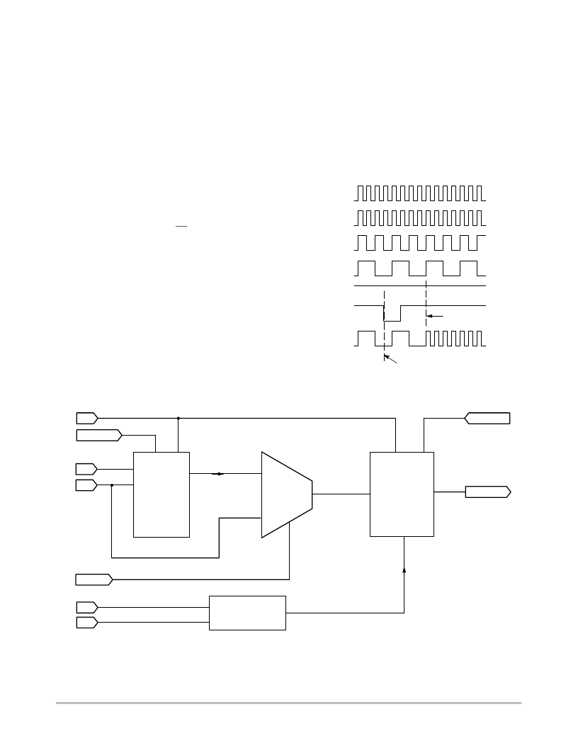
SMART CARD CLOCK DIVIDER
The main purpose of the built-in clock generator is
threefold:
1. Adapts the voltage level shifter to cope with the
different voltages that might exist between the
MPU and the Smart Card.
2. Provides a frequency division to adapt the Smart
Card operating frequency from the external clock
source.
3. Controls the clock state according to the smart
card specification.
In addition, the NCN6001 adjusts the signal coming from
the microprocessor to get the Duty Cycle window as defined
by the ISO7816-3 specification.
The byte content of the SPI port, B2 & B3, fulfills the
programming functions when CS is Low as depicted in
Figure 25 and Figure 24. The clock input stage (CLK_IN)
can handle a 20 MHz frequency maximum signal, the
divider being capable to provide a 1:4 ratio. Of course, the
ratio must be defined by the engineer to cope with the Smart
Card considered in a given application and, in any case, the
output clock [CRD_CLK] shall be limited to 20 MHz
maximum. In order to minimize the dI/dt and dV/dV
developed in the CRD_CLK line, the output stage includes
a special function to adapt the slope of the clock signal for
different applications
.
This function is programmed by the
MOSI register (Table 2: WRT_REG Bits Definitions and
Functions) whatever be the clock division.
In order to avoid any duty cycle out of the smart card
ISO7816-3 specification, the divider is synchronized by the
last flip flop, thus yielding a constant 50% duty cycle,
whatever be the divider ratio (Figure 24). Consequently, the
output CRD_CLK frequency division can be delayed by
four CLK_IN pulses and the microcontroller software must
take this delay into account prior to launch a new data
transaction. On the other hand, the output signal Duty Cycle
cannot be guaranteed 50% if the division ratio is 1 and if the
input Duty Cycle signal is not within the 46–56% range.
The input signals CLK_IN and MOSI/b3 are
automatically routed to the level shifter and control block
according to the mode of operation.
CRD_CLK
CLOCK_IN
CLOCK : 2
CLOCK : 4
B2
B3
Clock is updated upon
CLOCK: 4 rising edge
These bits program
CLOCK = 1:1 ratio
Internal
CLOCK
Divider
CLOCK programming is activated
by the B2 + B3 logic state
CLOCK : 1
Figure 24. Typical Clock Divider Synchronization
Figure 25. Basic Clock Divider and Level Shifter
B1
B0
B3
B2
CLK_IN
VCC
CRD_CLK
CRD_VCC
LEVEL SHIFTER
AND CONTROL
Programming
CRD_CLK Slope
NOTE: Bits [B0...B3] come from SPI data
Programming
CRD_CLK
Division
SYNC
ASYNC
SYNC
U1
DIGITAL_MUX
OUT
SEL
A
B
相關(guān)PDF資料 |
PDF描述 |
|---|---|
| NCN6004AFTBR2 | Dual SAM/SIM Interface Integrated Circuit |
| NCN6004A | Dual SAM/SIM Interface Integrated Circuit |
| NCN6010DTBR2 | SIM Card Supply and Level Shifter |
| NCN6010 | SIM Card Supply and Level Shifter |
| NCN6010D | SIM Card Supply and Level Shifter |
相關(guān)代理商/技術(shù)參數(shù) |
參數(shù)描述 |
|---|---|
| NCN6001/D | 制造商:ONSEMI 制造商全稱:ON Semiconductor 功能描述:Compact Smart Card Interface IC |
| NCN6001_06 | 制造商:ONSEMI 制造商全稱:ON Semiconductor 功能描述:Compact Smart Card Interface IC |
| NCN6001_0610 | 制造商:ONSEMI 制造商全稱:ON Semiconductor 功能描述:Smartcard Interface ICs |
| NCN6001DTBEVB | 功能描述:界面開(kāi)發(fā)工具 NCN6001 TSSOP EVAL BOARD RoHS:否 制造商:Bourns 產(chǎn)品:Evaluation Boards 類型:RS-485 工具用于評(píng)估:ADM3485E 接口類型:RS-485 工作電源電壓:3.3 V |
| NCN6001DTBR2 | 功能描述:輸入/輸出控制器接口集成電路 2.7V POS/ATM Smart RoHS:否 制造商:Silicon Labs 產(chǎn)品: 輸入/輸出端數(shù)量: 工作電源電壓: 最大工作溫度:+ 85 C 最小工作溫度:- 40 C 安裝風(fēng)格:SMD/SMT 封裝 / 箱體:QFN-64 封裝:Tray |
發(fā)布緊急采購(gòu),3分鐘左右您將得到回復(fù)。