- 您現(xiàn)在的位置:買賣IC網(wǎng) > PDF目錄359232 > MT88EBNR (ZARLINK SEMICONDUCTOR INC) 4-Wire Calling Number Identification Circuit 2 (4-Wire CNIC2) PDF資料下載
參數(shù)資料
| 型號: | MT88EBNR |
| 廠商: | ZARLINK SEMICONDUCTOR INC |
| 元件分類: | 無繩電話/電話 |
| 英文描述: | 4-Wire Calling Number Identification Circuit 2 (4-Wire CNIC2) |
| 中文描述: | TELEPHONE CALLING NO IDENT CKT, PDSO20 |
| 封裝: | 5.30 MM, MO-150AE, SSOP-20 |
| 文件頁數(shù): | 20/30頁 |
| 文件大小: | 523K |
| 代理商: | MT88EBNR |
第1頁第2頁第3頁第4頁第5頁第6頁第7頁第8頁第9頁第10頁第11頁第12頁第13頁第14頁第15頁第16頁第17頁第18頁第19頁當前第20頁第21頁第22頁第23頁第24頁第25頁第26頁第27頁第28頁第29頁第30頁
MT88E45
Data Sheet
20
Zarlink Semiconductor Inc.
AC Electrical Characteristics are over recommended operating conditions, unless otherwise stated.
Typical figures are nominal values and are for design aid only: not guaranteed and not subject to production testing.
*Notes:
1. Both mark and space have the same amplitude.
2. Tip/Ring signal level. Input op-amp configured to 0dB gain at Vdd=5V+/-10%, -3.5dB at Vdd=3V+/-10%.
3. Band limited random noise (200-3400Hz). Present when FSK signal is present. Note that the BT band is 300-3400Hz, the Bellcore
band is 0-4kHz.
4. dBV - Decibels above or below a reference voltage of 1 Vrms. 0 dBV = 1 Vrms.
5. dBm - Decibels above or below a reference power of 1 mW into 600 ohms. 0 dBm = 0.7746 Vrms.
Electrical characteristics are over recommended operating conditions, unless otherwise stated.
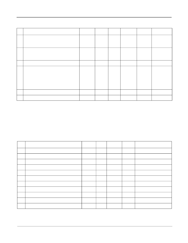
AC Electrical Characteristics
- FSK Demodulation
Characteristics
Sym.
Min.
Typ.
Max.
Units
Notes*
1
Accept Signal Level Range
-40
-37.78
10.0
-6.45
-4.23
476
dBV
dBm
mVrms
1, 2, 4, 5
2
Bell 202 Format Reject Signal Level
-48.24
-50.46
3
dBm
dBV
mVrms
1, 2, 4, 5
3
Transmission Rate
1188
1200
1212
baud
4
Mark and Space Frequencies
Bell 202 1 (Mark)
Bell 202 0 (Space)
CCITT V.23 1 (Mark)
CCITT V.23 0 (Space)
1188
2178
1280.5
2068.5
1200
2200
1300
2100
1212
2222
1319.5
2131.5
Hz
Hz
Hz
Hz
5
Twist: 20 log (V
MARK
/V
SPACE
)
-6
+10
dB
6
Signal to Noise Ratio
SNR
FSK
20
dB
1,3
Electrical Characteristics
- Gain Setting Amplifiers
Characteristics
Sym.
Min.
Max.
Units
Test Conditions
1
Input Leakage Current
I
IN
1
μ
A
V
SS
≤
V
IN
≤
V
DD
2
Input Resistance
R
in
10
M
3
Input Offset Voltage
V
OS
25
mV
4
Power Supply Rejection Ratio
PSRR
30
dB
1kHz ripple on V
DD
V
CMmin
≤
V
IN
≤
V
CMmax
5
Common Mode Rejection Ratio
CMRR
40
dB
6
DC Open Loop Voltage Gain
A
VOL
40
dB
7
Unity Gain Bandwidth
f
C
0.3
MHz
8
Output Voltage Swing
V
O
0.5
V
DD
-0.5
V
Load
≥
100k
9
Capacitive Load (GS1,GS2)
C
L
50
pF
10
Resistive Load (GS1,GS2)
R
L
100
k
11
Common Mode Range Voltage
V
CM
1.0
V
DD
-1.0
V
相關(guān)PDF資料 |
PDF描述 |
|---|---|
| MT88L70AE1 | 3 Volt Integrated DTMF Receiver |
| MT88L70AE | 3 Volt Integrated DTMF Receiver |
| MT88L70AN | 3 Volt Integrated DTMF Receiver |
| MT88L70AN1 | 3 Volt Integrated DTMF Receiver |
| MT88L70ASR | 3 Volt Integrated DTMF Receiver |
相關(guān)代理商/技術(shù)參數(shù) |
參數(shù)描述 |
|---|---|
| MT88L70 | 制造商:ZARLINK 制造商全稱:Zarlink Semiconductor Inc 功能描述:3 Volt Integrated DTMF Receiver |
| MT88L70AC | 制造商:MITEL 制造商全稱:Mitel Networks Corporation 功能描述:3 Volt Integrated DTMF Receiver |
| MT88L70AE | 制造商:Microsemi Corporation 功能描述: |
| MT88L70AE1 | 制造商:Microsemi Corporation 功能描述:DTMF RX 3.58MHZ CMOS 3V 18PDIP - Rail/Tube |
| MT88L70AN | 制造商:Microsemi Corporation 功能描述: |
發(fā)布緊急采購,3分鐘左右您將得到回復(fù)。