- 您現(xiàn)在的位置:買賣IC網(wǎng) > PDF目錄385639 > MT46V32M4TG-8 (Micron Technology, Inc.) DOUBLE DATA RATE DDR SDRAM PDF資料下載
參數(shù)資料
| 型號: | MT46V32M4TG-8 |
| 廠商: | Micron Technology, Inc. |
| 英文描述: | DOUBLE DATA RATE DDR SDRAM |
| 中文描述: | 雙倍數(shù)據(jù)速率的DDR SDRAM內存 |
| 文件頁數(shù): | 52/68頁 |
| 文件大?。?/td> | 2547K |
| 代理商: | MT46V32M4TG-8 |
第1頁第2頁第3頁第4頁第5頁第6頁第7頁第8頁第9頁第10頁第11頁第12頁第13頁第14頁第15頁第16頁第17頁第18頁第19頁第20頁第21頁第22頁第23頁第24頁第25頁第26頁第27頁第28頁第29頁第30頁第31頁第32頁第33頁第34頁第35頁第36頁第37頁第38頁第39頁第40頁第41頁第42頁第43頁第44頁第45頁第46頁第47頁第48頁第49頁第50頁第51頁當前第52頁第53頁第54頁第55頁第56頁第57頁第58頁第59頁第60頁第61頁第62頁第63頁第64頁第65頁第66頁第67頁第68頁
52
128Mb: x4, x8, x16 DDR SDRAM
128Mx4x8x16DDR_C.p65
–
Rev. C; Pub. 4/01
Micron Technology, Inc., reserves the right to change products or specifications without notice.
2001, Micron Technology, Inc.
128Mb: x4, x8, x16
DDR SDRAM
PRELIMINARY
NOTES (continued)
32. V
DD
must not vary more than 4% if CKE is not
active while any bank is active.
33. The clock is allowed up to ±150ps of jitter. Each
timing parameter is allowed to vary by the same
amount.
34.
t
HP min is the lesser of
t
CL minimum and
t
CH
minimum actually applied to the device CK and
CK/ inputs, collectively during bank active.
35. READs and WRITEs with auto precharge are not
allowed to be issued until
t
RAS
(MIN)
can be
satisfied prior to the internal precharge com-
mand being issued.
36. Any positive glitch must be less than
1
/
3
of the
clock and not more than +400mV or 2.9 volts,
whichever is less. Any negative glitch must be less
than
1
/
3
of the clock cycle and not exceed either
-300mV or 2.2 volts, whichever is more positive.
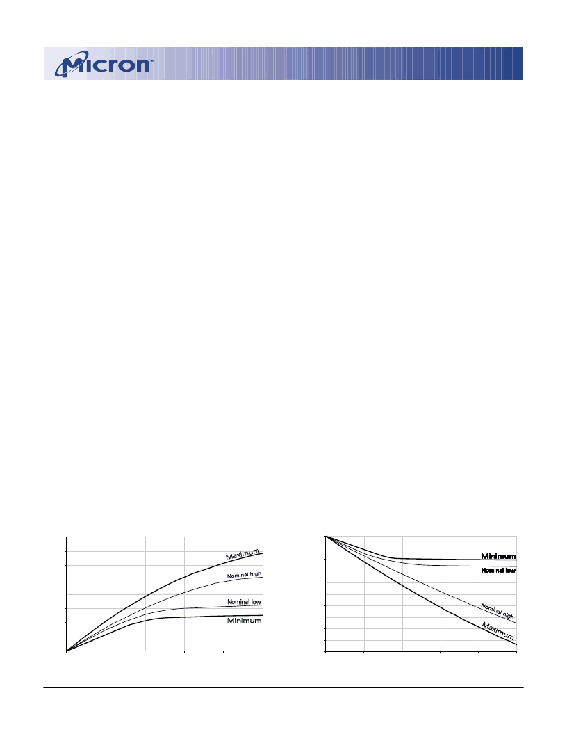
37. Normal Output Drive Curves:
a)The full variation in driver pull-down current
from minimum to maximum process, tem-
perature and voltage will lie within the outer
bounding lines of the V-I curve of Figure A.
b)The variation in driver pull-down current
within nominal limits of voltage and tempera-
ture is expected, but not guaranteed, to lie
within the inner bounding lines of the V-I
curve of Figure A.
c) The full variation in driver pull-up current
from minimum to maximum process,
temperature and voltage will lie within the
outer bounding lines of the V-I curve of
Figure B.
d)The variation in driver pull-up current within
nominal limits of voltage and temperature is
expected, but not guaranteed, to lie within
the inner bounding lines of the V-I curve of
Figure B.
e) The full variation in the ratio of the maximum
to minimum pull-up and pull-down current
should be between .71 and 1.4, for device
drain-to-source voltages from 0.1V to 1.0 Volt,
and at the same voltage and temperature.
f) The full variation in the ratio of the nominal
pull-up to pull-down current should be unity
±10%, for device drain-to-source voltages
from 0.1V to 1.0 Volt.
38. Reduced Output Drive Curves:
a)The full variation in driver pull-down current
from minimum to maximum process, tem-
perature and voltage will lie within the outer
bounding lines of the V-I curve of Figure C.
b)The variation in driver pull-down current
within nominal limits of voltage and tempera-
ture is expected, but not guaranteed, to lie
within the inner bounding lines of the V-I
curve of Figure C.
c) The full variation in driver pull-up current
from minimum to maximum process, tempera-
ture and voltage will lie within the outer
bounding lines of the V-I curve of Figure D.
d)The variation in driver pull-up current within
nominal limits of voltage and temperature is
expected, but not guaranteed, to lie within
the inner bounding lines of the V-I curve of
Figure D.
e) The full variation in the ratio of the maximum
to minimum pull-up and pull-down current
should be between .71 and 1.4, for device
drain-to-source voltages from 0.1V to 1.0 V,
and at the same voltage.
f) The full variation in the ratio of the nominal
pull-up to pull-down current should be unity
±10%, for device drain-to-source voltages
from 0.1V to 1.0 V.
Figure B
Pull-Up Characteristics
-200
-180
-160
-140
-120
-100
-80
-60
-40
-20
0
0.0
0.5
1.0
1.5
2.0
2.5
I
O
V
DD
Q - V
OUT
(V)
Figure A
Pull-Down Characteristics
0
20
40
60
80
100
120
140
160
0.0
0.5
1.0
1.5
2.0
2.5
V
OUT
(V)
I
O
相關PDF資料 |
PDF描述 |
|---|---|
| MT46V32M4TG-8L | DOUBLE DATA RATE DDR SDRAM |
| MT46V4M32 | DOUBLE DATA RATE DDR SDRAM |
| MT46V4M32LG | I.MX31 LITE KIT |
| MT46V64M4 | 16 Meg x 4 x 4 banks DDR SDRAM(16M x 4 x 4組,雙數(shù)據(jù)速率同步動態(tài)RAM) |
| MT46V64M8 | 16 Meg x 8 x 4 banks DDR SDRAM(16M x 8 x 4組,雙數(shù)據(jù)速率同步動態(tài)RAM) |
相關代理商/技術參數(shù) |
參數(shù)描述 |
|---|---|
| MT46V32M4TG-8L | 制造商:MICRON 制造商全稱:Micron Technology 功能描述:DOUBLE DATA RATE DDR SDRAM |
| MT46V32M8 | 制造商:MICRON 制造商全稱:Micron Technology 功能描述:DOUBLE DATA RATE DDR SDRAM |
| MT46V32M82ZZ5-75 ES | 制造商:Micron Technology Inc 功能描述:32MX8 SDRAM DDR PLASTIC PBF FBGA 2.5V - Trays |
| MT46V32M82ZZ5-75EZ | 制造商:Micron Technology Inc 功能描述:32MX8 DDR SDRAM PLASTIC 2.5V - Trays |
發(fā)布緊急采購,3分鐘左右您將得到回復。