- 您現(xiàn)在的位置:買賣IC網(wǎng) > PDF目錄378013 > MSM548262-70TS-K (OKI SEMICONDUCTOR CO., LTD.) 262,144-Word x 8-Bit Multiport DRAM PDF資料下載
參數(shù)資料
| 型號: | MSM548262-70TS-K |
| 廠商: | OKI SEMICONDUCTOR CO., LTD. |
| 英文描述: | 262,144-Word x 8-Bit Multiport DRAM |
| 中文描述: | 262,144字× 8位多端口內(nèi)存 |
| 文件頁數(shù): | 33/37頁 |
| 文件大?。?/td> | 464K |
| 代理商: | MSM548262-70TS-K |
第1頁第2頁第3頁第4頁第5頁第6頁第7頁第8頁第9頁第10頁第11頁第12頁第13頁第14頁第15頁第16頁第17頁第18頁第19頁第20頁第21頁第22頁第23頁第24頁第25頁第26頁第27頁第28頁第29頁第30頁第31頁第32頁當(dāng)前第33頁第34頁第35頁第36頁第37頁
Semiconductor
MSM548262
33/37
DATA TRANSFER OPERATIONS
The MSM548262 features two types of bidirectional data transfer capability between RAM and
SAM.
1) Conventional (non split) transfer: 512 words by 8 bits of data can be loaded from RAM to SAM
(Read transfer), or from SAM to RAM (Write transfer).
2) Split transfer: 256 words by 8 bits of data can be loaded from the lower/upper half of the RAM
to the lower/upper half of the SAM (Split read transfer), or from the lower/upper half of SAM
to the lower/upper half of RAM (Split write transfer).
The conventional transfer and split transfer modes are controlled by the DSF input signal.
Data transfer are invoked by holding the
TRG
signal "low" at the falling edge of
RAS
.
The MSM548262 supports 4 types of transfer operations: Read transfer, Split read transfer, Write
transfer and Split write transfer as shown in the truth table. The type of transfer operation is
determined by the state of
CAS
,
WE
and DSF latched at the falling edge of
RAS
. During
conventional transfer operations, the SAM port is switched from input to output mode (Read
transfer), or output to input mode (Write transfer). It remains unchanged during split transfer
operation (Split read transfer or Split write transfer).
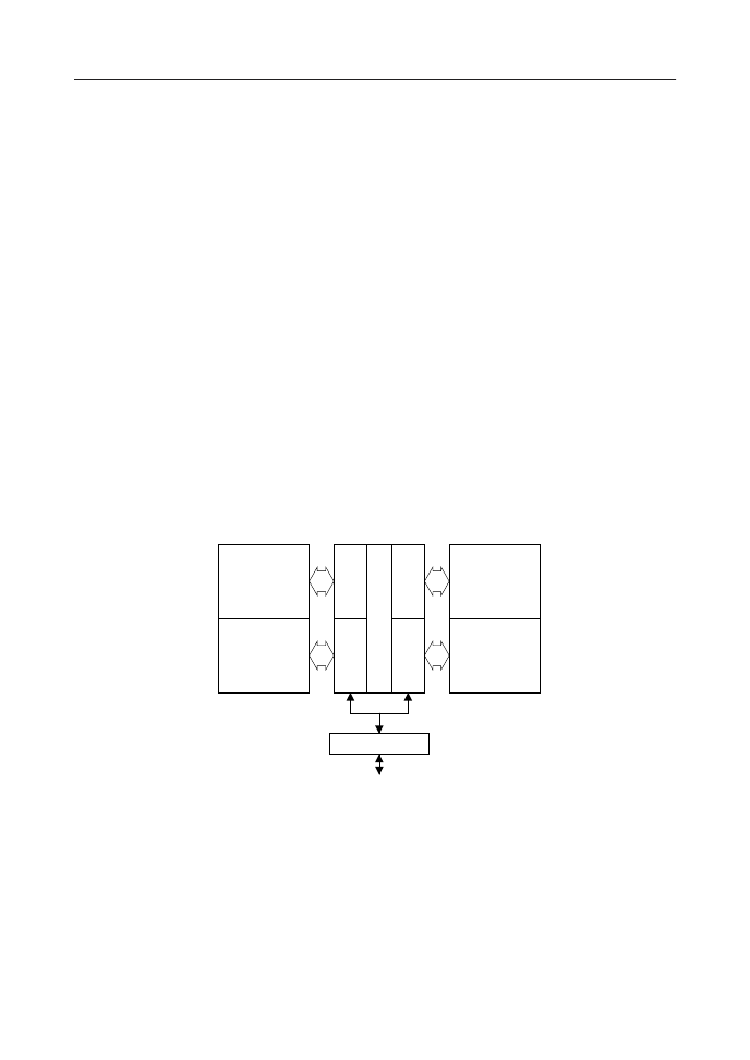
Both RAM and SAM are divided by the most significant row address (AX8), as shown in Figure
1. Therefore, no data transfer between AX8 = 0 side RAM and AX8 = 1 side RAM can be provided
through the SAM. Care must be taken if the split read transfer on AX8 = 1 side (or AX8 = 0 side)
is provided after the read transfer or the split read transfer, is provided on AX8 = 0 side (or AX8
= 1 side).
Figure 1. RAM and SAM Configuration
256
¥
256
¥
8
Memory
Array
256
¥
256
¥
8
Memory
Array
256
¥
256
¥
8
Memory
Array
256
¥
256
¥
8
Memory
Array
S
U
2
¥
L
2
¥
U
2
¥
L
2
¥
AX8 = 0
AX8 = 1
SAM I/O Buffer
SDQ1 - 8
相關(guān)PDF資料 |
PDF描述 |
|---|---|
| MSM548262-80JS | 262,144-Word x 8-Bit Multiport DRAM |
| MSM548262-80TS-K | 262,144-Word x 8-Bit Multiport DRAM |
| MSM548262 | 262,144-Word ×8-Bit Multiport DRAM(256k字×8位多端口動態(tài)RAM) |
| MSM548263 | 262,144-Word ×8-Bit Multiport DRAM(256k字×8位多端口動態(tài)RAM) |
| MSM548512L-XXGS-K | 524,288-Word X 8-Bit High-Speed PSRAM |
相關(guān)代理商/技術(shù)參數(shù) |
參數(shù)描述 |
|---|---|
| MSM548262-JS70 | 制造商:ROHM Semiconductor 功能描述: |
| MSM548263-60JS | 制造商:ROHM Semiconductor 功能描述: |
| MSM548263-60TS-K | 制造商:OK International 功能描述: |
| MSM54V12222A-30TS-K | 制造商:OKI Semiconductor 功能描述:FIELD/FRAME/LINE MEMORY, 44 Pin, Plastic, TSOP |
| MSM54V12222B-25JDR17 | 制造商:ROHM Semiconductor 功能描述: |
發(fā)布緊急采購,3分鐘左右您將得到回復(fù)。