- 您現(xiàn)在的位置:買賣IC網(wǎng) > PDF目錄69037 > MPC972FA (FREESCALE SEMICONDUCTOR INC) 125 MHz, PROC SPECIFIC CLOCK GENERATOR, PQFP52 PDF資料下載
參數(shù)資料
| 型號(hào): | MPC972FA |
| 廠商: | FREESCALE SEMICONDUCTOR INC |
| 元件分類: | 時(shí)鐘產(chǎn)生/分配 |
| 英文描述: | 125 MHz, PROC SPECIFIC CLOCK GENERATOR, PQFP52 |
| 封裝: | LQFP-52 |
| 文件頁(yè)數(shù): | 8/12頁(yè) |
| 文件大小: | 337K |
| 代理商: | MPC972FA |
MPC972
MOTOROLA ADVANCED CLOCK DRIVERS DEVICE DATA
190
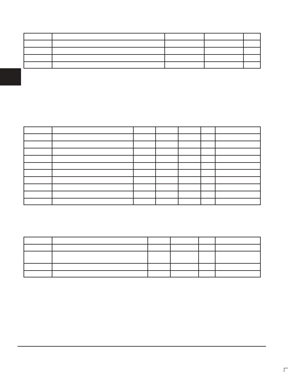
ABSOLUTE MAXIMUM RATINGS*
Symbol
Parameter
Min
Max
Unit
VCC
Supply Voltage
–0.3
4.6
V
VI
Input Voltage
–0.3
VCC + 0.3
V
IIN
Input Current
±20
mA
TStor
Storage Temperature Range
–40
125
°C
* Absolute maximum continuous ratings are those values beyond which damage to the device may occur. Exposure to these conditions or condi-
tions beyond those indicated may adversely affect device reliability. Functional operation under absolute-maximum-rated conditions is not im-
plied.
THERMAL CHARACTERISTICS
Proper thermal management is critical for reliable system operation. This is especially true for high fanout and high drive capa-
bility products. Generic thermal information is available for the Motorola Clock Driver products. The means of calculating die
power, the corresponding die temperature and the relationship to long–term reliability is addressed in the Motorola application
note AN1545.
DC CHARACTERISTICS (Note 3.; TA = 0° to 70°C; VCC = 3.3 V ±5%)
Symbol
Characteristic
Min
Typ
Max
Unit
Condition
VCCA
Analog VCC Voltage
2.935
VCC
V
VIH
Input HIGH Voltage
2.0
3.6
V
VIL
Input LOW Voltage
0.8
V
VOH
Output HIGH Voltage
2.4
V
IOH = –20 mA (Note 1.)
VOL
Output LOW Voltage
0.5
V
IOL = 20 mA (Note 1.)
IIN
Input Current
±120
A
Note 2.
ICC
Maximum Quiescent Supply Current
190
215
mA
All VCC PIns
ICCA
Analog VCC Current
15
20
mA
CIN
Input Capacitance
4
pF
Cpd
Power Dissipation Capacitance
25
pF
Per Output
1. The MPC972 outputs can drive series or parallel terminated 50
(or 50 to VCC/2) transmission lines on the incident edge (see Applications
Info section).
2. Inputs have pull–up/pull–down resistors which affect input current.
3. Special thermal handling may be required in some configurations.
PLL INPUT REFERENCE CHARACTERISTICS (TA = 0° to 70°C)
Symbol
Characteristic
Min
Max
Unit
Condition
tr, tf
TCLK Input Rise/Falls
3.0
ns
fref
Reference Input Frequency
Note 1.
100
Note 1.
MHz
frefDC
Reference Input Duty Cycle
25
75
%
txtal
Crystal Oscillator Frequency
10
25
MHz
Note 2.
1. Maximum input reference frequency is limited by the VCO lock range and the feedback divider or 100MHz, minimum input reference frequency
is limited by the VCO lock range and the feedback divider.
2. See Applications Info section for more crystal information.
2
F
re
e
sc
a
le
S
e
m
ic
o
n
d
u
c
to
r,
I
Freescale Semiconductor, Inc.
For More Information On This Product,
Go to: www.freescale.com
n
c
..
.
相關(guān)PDF資料 |
PDF描述 |
|---|---|
| MPC9850VF | 500 MHz, PROC SPECIFIC CLOCK GENERATOR, PBGA100 |
| MPC9850VMR2 | 500 MHz, PROC SPECIFIC CLOCK GENERATOR, PBGA100 |
| MPC9850VMR2 | 500 MHz, PROC SPECIFIC CLOCK GENERATOR, PBGA100 |
| MPC9850VFR2 | 500 MHz, PROC SPECIFIC CLOCK GENERATOR, PBGA100 |
| MPC9992FAR2 | 400 MHz, OTHER CLOCK GENERATOR, PQFP32 |
相關(guān)代理商/技術(shù)參數(shù) |
參數(shù)描述 |
|---|---|
| MPC972H10 F44A WAF | 制造商:Motorola Inc 功能描述: |
| MPC973 | 制造商:MOTOROLA 制造商全稱:Motorola, Inc 功能描述:LOW VOLTAGE PLL CLOCK DRIVER |
| MPC974 | 制造商:MOTOROLA 制造商全稱:Motorola, Inc 功能描述:LOW VOLTAGE PLL CLOCK DRIVER |
| MPC974A44 F44A WAF | 制造商:Motorola Inc 功能描述: |
| MPC9772 | 制造商:MOTOROLA 制造商全稱:Motorola, Inc 功能描述:3.3V 1:12 LVCMOS PLL Clock Generator |
發(fā)布緊急采購(gòu),3分鐘左右您將得到回復(fù)。