- 您現(xiàn)在的位置:買賣IC網(wǎng) > PDF目錄69037 > MPC972FA (FREESCALE SEMICONDUCTOR INC) 125 MHz, PROC SPECIFIC CLOCK GENERATOR, PQFP52 PDF資料下載
參數(shù)資料
| 型號(hào): | MPC972FA |
| 廠商: | FREESCALE SEMICONDUCTOR INC |
| 元件分類: | 時(shí)鐘產(chǎn)生/分配 |
| 英文描述: | 125 MHz, PROC SPECIFIC CLOCK GENERATOR, PQFP52 |
| 封裝: | LQFP-52 |
| 文件頁數(shù): | 4/12頁 |
| 文件大小: | 337K |
| 代理商: | MPC972FA |
MPC972
MOTOROLA ADVANCED CLOCK DRIVERS DEVICE DATA
197
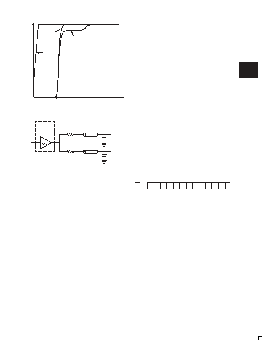
Figure 13. Single versus Dual Waveforms
TIME (nS)
VOL
TAGE
(V)
3.0
2.5
2.0
1.5
1.0
0.5
0
2
4
6
8
10
12
14
OutB
tD = 3.9386
OutA
tD = 3.8956
In
Figure 14. Optimized Dual Line Termination
7
MPC972
OUTPUT
BUFFER
RS = 36
ZO = 50
RS = 36
ZO = 50
7
+ 36 k 36 = 50 k 50
25
= 25
SPICE level output buffer models are available for engineers
who want to simulate their specific interconnect schemes. In
addition IV characteristics are in the process of being generated
to support the other board level simulators in general use.
Using the Output Freeze Circuitry
With the recent advent of a “green” classification for
computers the desire for unique power management among
system designers is keen. The individual output enable control
of the MPC972 allows designers, under software control, to
implement unique power management schemes into their
designs. Although useful, individual output control at the
expense of one pin per output is too high, therefore a simple
serial interface was derived to economize on the control pins.
The freeze control logic provides a mechanism through which
the MPC972 clock outputs may be frozen (stopped in the logic
‘0’ state):
The freeze mechanism allows serial loading of the 12–bit
Serial Input Register, this register contains one programmable
freeze enable bit for 12 of the 14 output clocks. The Qc0 and
QFB outputs cannot be frozen with the serial port, this avoids
any potential lock up situation should an error occur in the
loading of the Serial Input Register. The user may program an
output clock to freeze by writing logic ‘0’ to the respective freeze
enable bit. Likewise, the user may programmably unfreeze an
output clock by writing logic ‘1’ to the respective enable bit.
The freeze logic will never force a newly–frozen clock to a
logic ‘0’ state before the time at which it would normally
transition there. The logic simply keeps the frozen clock at logic
‘0’ once it is there. Likewise, the freeze logic will never force a
newly–unfrozen clock to a logic ‘1’ state before the time at which
it would normally transition there. The logic re–enables the
unfrozen clock during the time when the respective clock would
normally be in a logic ‘0’ state, eliminating the possibility of ‘runt’
clock pulses.
The user may write to the Serial Input register through the
Frz_Data input by supplying a logic ‘0’ start bit followed serially
by 12 NRZ freeze enable bits. The period of each Frz_Data bit
equals the period of the free–running Frz_Clk signal. The
Frz_Data serial transmission should be timed so the MPC972
can sample each Frz_Data bit with the rising edge of the
free–running Frz_Clk signal.
Figure 15. Freeze Data Input Protocol
D1 D2 D3 D4 D5 D6 D7 D8 D9 D10 D11
D0
Start
Bit
D0-D3 are the control bits for Qa0-Qa3, respectively
D4-D7 are the control bits for Qb0-Qb3, respectively
D8-D10 are the control bits for Qc1-Qc3, respectively
D11 is the control bit for QSync
2
F
re
e
sc
a
le
S
e
m
ic
o
n
d
u
c
to
r,
I
Freescale Semiconductor, Inc.
For More Information On This Product,
Go to: www.freescale.com
n
c
..
.
相關(guān)PDF資料 |
PDF描述 |
|---|---|
| MPC9850VF | 500 MHz, PROC SPECIFIC CLOCK GENERATOR, PBGA100 |
| MPC9850VMR2 | 500 MHz, PROC SPECIFIC CLOCK GENERATOR, PBGA100 |
| MPC9850VMR2 | 500 MHz, PROC SPECIFIC CLOCK GENERATOR, PBGA100 |
| MPC9850VFR2 | 500 MHz, PROC SPECIFIC CLOCK GENERATOR, PBGA100 |
| MPC9992FAR2 | 400 MHz, OTHER CLOCK GENERATOR, PQFP32 |
相關(guān)代理商/技術(shù)參數(shù) |
參數(shù)描述 |
|---|---|
| MPC972H10 F44A WAF | 制造商:Motorola Inc 功能描述: |
| MPC973 | 制造商:MOTOROLA 制造商全稱:Motorola, Inc 功能描述:LOW VOLTAGE PLL CLOCK DRIVER |
| MPC974 | 制造商:MOTOROLA 制造商全稱:Motorola, Inc 功能描述:LOW VOLTAGE PLL CLOCK DRIVER |
| MPC974A44 F44A WAF | 制造商:Motorola Inc 功能描述: |
| MPC9772 | 制造商:MOTOROLA 制造商全稱:Motorola, Inc 功能描述:3.3V 1:12 LVCMOS PLL Clock Generator |
發(fā)布緊急采購(gòu),3分鐘左右您將得到回復(fù)。